I built a Game Boy and Game Boy Color emulator that runs on an FPGA, and can play both physical cartridges and ROM files. The whole project took about 4 months of intermittent work.
Check out the code and instructions for running it here.
Update February 2025: I expanded this project into a standalone, handheld device and added GBA support.
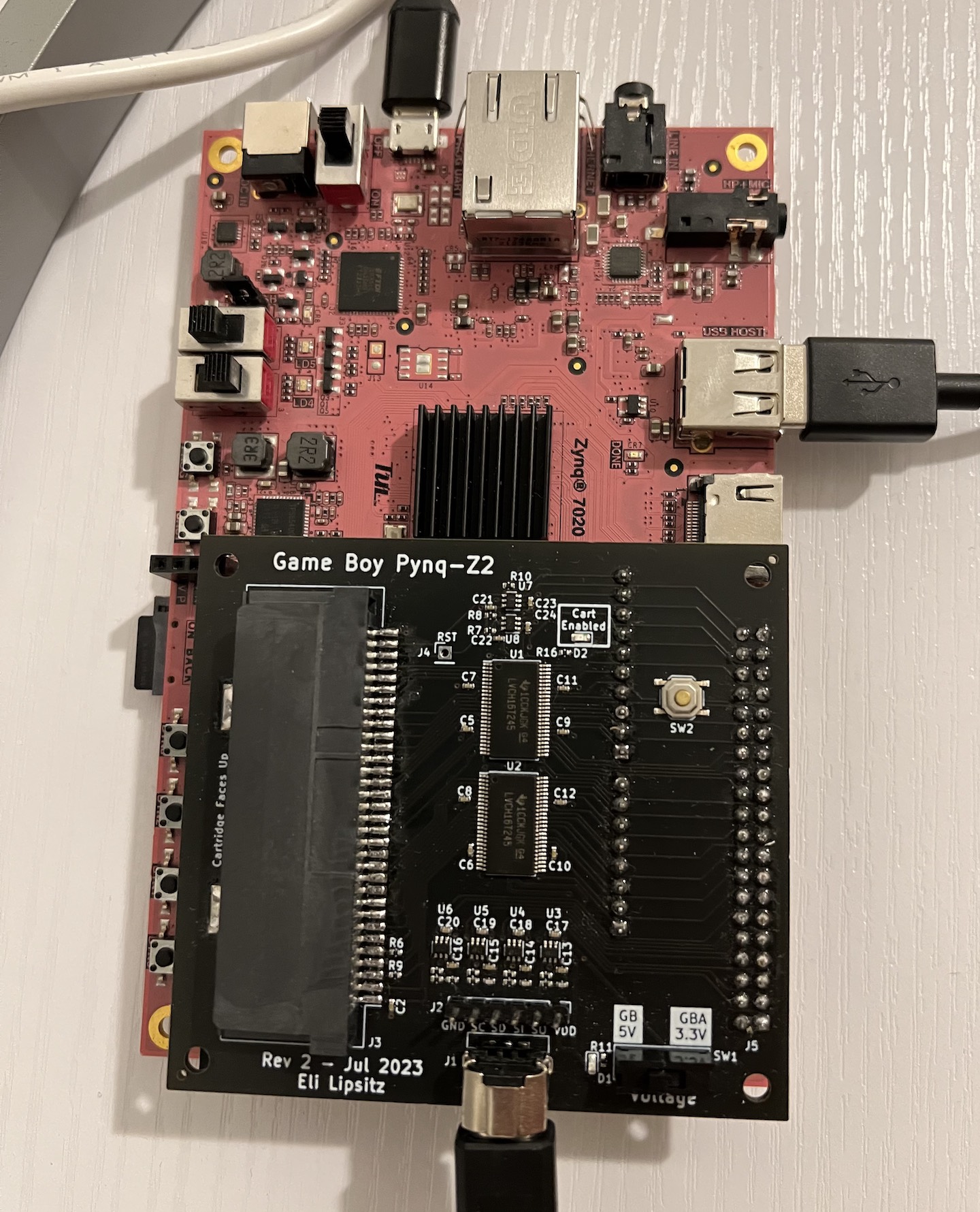
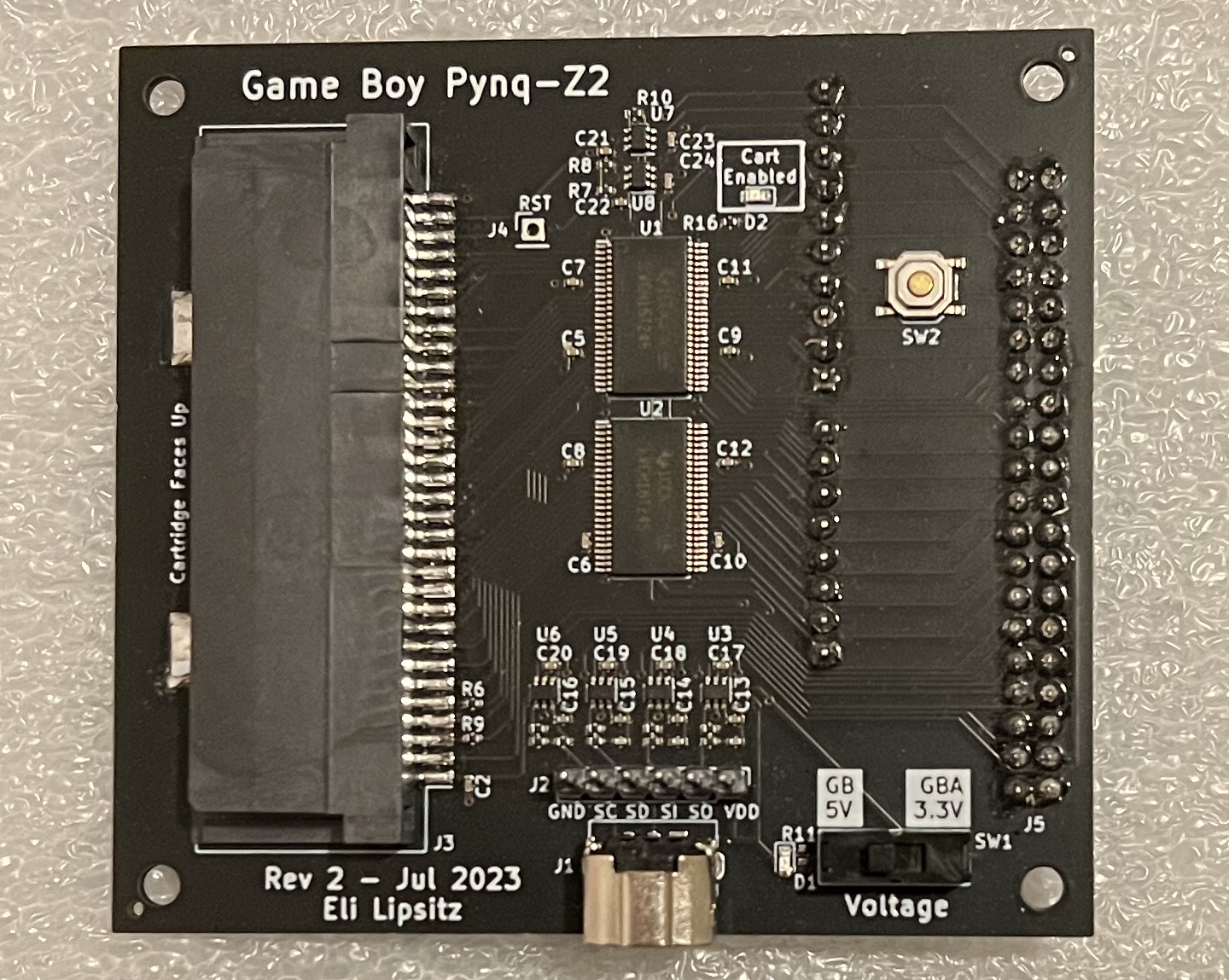
Assembled FPGA board with cartridge adapter
Introduction
I’ve written a few video game system emulators before. My very first one was a mostly-complete NES emulator written in Go. Later, when I was learning Rust, I wrote another, better NES emulator in Rust. Then, in late 2021, I decided I wanted to write an emulator for a system I had a closer personal connection to, so I wrote a Game Boy Advance emulator.
This time, I wanted to try something different. All of my previous emulators were software emulators — nearly all video game emulators are. They’re computer programs that run and interpret the game code, and simulate how various components of the system (e.g. CPU, graphics, sound) interact together. All of this runs entirely in software on a host computer. Other emulators are hardware emulators, where the emulator is an actual piece of hardware. The idea is the same (create something that isn’t the original hardware that, in some way, behaves like the original hardware), but the implementation is different. In particular, you could have an FPGA configured to behave like one or more integrated circuits from the original hardware.
Despite what some people claim, an FPGA-based emulator is still an emulator, since it’s an imitation of the original system. Furthermore, FPGA-based emulators aren’t inherently more accurate than a software-based emulator. In fact, they have a whole set of disadvantages (cost, ease of implementation). However, they have one notable advantage over a software emulator running on a PC: timing and hardware interfaces.
An FPGA can easily emulate the exact timing of the original system, which enables an FPGA-based emulator to interact with physical hardware, such as game cartridges, input devices, or other systems (e.g. another game console over a multiplayer link cable). A software emulator running on a modern host computer could never achieve the latency required to do this. For example, the Game Boy accesses the cartridge at 1 MHz, so every microsecond the emulator would have to stop, interface with an external hardware device, and then keep going. Desktop operating systems do not allow that level of control over scheduling, and modern computers don’t generally have external low-latency, low-level I/O interfaces. USB 2.0 has a theoretical minimum latency of 125 microseconds, and USB 3.0 could maybe get down to 50 microseconds or so. Either way, a far cry from the sub-microsecond latency required to interface with a Game Boy cartridge.
A software emulator running on a microcontroller might be able to hit timing and hardware interface requirements. You don’t get the precise timing “for free” like you would with an FPGA, but you get a simpler programming model (pretty much the same as a software emulator running on a desktop computer).
I had been wanting to play around with FPGAs for a while, and I thought it would be an interesting challenge to write an emulator using one. When I wrote my other emulators, there were some behaviors (e.g. how registers were laid out, or the timing of certain operations) that hinted at the underlying hardware implementation, and I was interested in experiencing this firsthand by implementing the hardware myself.
There are already few FPGA emulator projects out there. Aside from various Game Boy emulators that people have written in Verilog, there’s the open-source MiSTER project that emulates 30+ different systems on the Terasic DE10-Nano board, featuring an Intel Cyclone V FPGA. MiSTER is a very impressive project, with excellent compatibility, features, and a large community. There’s also the Analogue Pocket, a commercial handheld device that emulates a few systems officially (including Game Boy and Game Boy Advance), and allows third party developers to write their own emulators for the device.
Goals
I set out a few goals for the project. I wanted to create a fully functional Game Boy emulator running on an FPGA, with very good game compatibility and high accuracy (though not necessarily 100%).
The emulator should be fully interactive, supporting a game controller as an input device, and with audio and video output. I wanted to be able to use real game cartridges, and to connect to another physical Game Boy via a Game Link Cable (after all, what’s to differentiate this from any other emulator project). This would involve a little bit of electrical engineering and PCB design to be able to connect a cartridge and link cable to the FPGA.
I also didn’t want to restrict myself to physical cartridges. Ideally, I’d be able to play ROM files on the emulator too. This would include some sort of on-device menu to be able to select the game to play.
And of course, I wanted to have fun and gain some experience using FPGAs.
FPGAs: What and How
Hardware Description Languages
FPGAs use a very different programming model from software. With a conventional programming language, you describe the flow of program execution. For an FPGA (or an ASIC), you use a hardware description language (HDL) to describe the structure of the digital logic circuit. Essentially, you’re designing a state machine by putting together combinatorial logic and sequential logic, with parallelism bounded only by the size of the FPGA.
The most commonly used HDLs are Verilog / SystemVerilog and VHDL. I used Verilog when I first started this project. Unfortunately, Verilog isn’t a great language. It’s pretty old, missing a lot of modern language features, and it has a number of footguns that can result in unexpected behavior.
Fortunately, Verilog (and VHDL) is no longer the only option. While vendor tooling generally requires one of these as inputs, there are a number of higher-level HDLs that compile down to Verilog. Chisel, SpinalHDL, and Migen are some of the most well-known examples. It’s important to note that these are higher-level HDLs, HDLs that compile down to another HDL. This is very different from the similarly named high-level synthesis, another technique that aims to allow designers to write in a conventional programming language such as C, and automatically generate hardware with matching behavior.
After researching the options a little bit, I decided to give Chisel a try. Chisel allows you to describe your hardware using DSL in Scala. Chisel seemed to be the most widely used of these higher-level HDLs, it looked pleasant to use, and does away with the footguns of Verilog. Plus, it was created at my alma mater. Using a higher-level HDL adds an extra layer of abstraction to debug, but from my experience in this project, using Chisel had way more benefits than drawbacks.
Simulation
Most FPGA development happens without ever interacting with an FPGA. Instead, developers use simulators as much as possible, for a few reasons. First, simulators allow you to easily write automated testbenches. Second, debugging a physical FPGA is significantly harder than debugging in a simulator (where you can add print statements and easily inspect all internal state). Finally, “compiling” (synthesis and place-and-route) for an FPGA is a slow process, taking a few minutes for small designs, and up to hours or even days for very large designs.
I used the ChiselTest library for small test benches, and used Verilator to run the complete emulator. Verilator is an interesting piece of software: it translates a Verilog desig into a C++ simulation for improved performance.
FPGA Development Boards
Before you can run your design on an FPGA, you have to pick an actual FPGA to use. There are a few FPGA vendors out there, but the two that produce the largest FPGAs are Xilinx (AMD) and Altera (Intel). I decided to pick up a Pynq-Z2, a development board centered around the Xilinx Zynq XC7Z020. I choose this one for a few reasons:
- Xilinx tooling (Vivado) seemed better than Altera tooling (Quartus)
- The board was capable of HDMI output
- The FPGA was large enough for my needs
- It was relatively inexpensive — only $120
- Zynq combines an FPGA and microprocessor onto an SoC
On that last point: the FPGA on the board can be programmed and used as a standalone FPGA, but it also bundles two ARM cores and enough DRAM to run Linux. The FPGA (in Xilinx terminology, the “PL — programmable logic”) and microprocessor (the “PS — processing system”) have high-speed interconnects. I planned to dedicate the FPGA to running the emulator (and producing audio/video output) and use the Linux system to program the FPGA, load ROMs from a microSD card, and handle gamepad input.
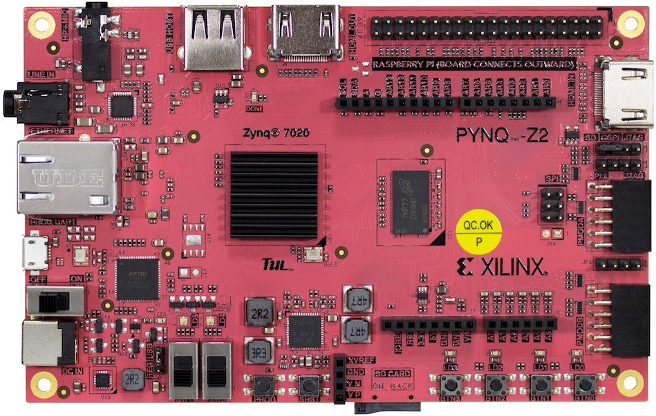
Pynq-Z2 development board
Running on an FPGA
To compile the Verilog output of the Chisel compiler into a “bitstream” that you can program onto an FPGA, you need to do “synthesis” and “place-and-route”. Synthesis is the process of converting Verilog into a list of FPGA resources (look-up-tables, flip flops, memories, I/O buffers) and their connections. Place-and-route takes this list and figures out how to map the logical resources to the physical resources present on a specific FPGA chip (“place”), and connect all of these resources together using the chip’s interconnects (“route”). For my final emulator design, the whole FPGA compilation process took about 25 minutes, compared to 45 seconds to build the simulator.
Modern FPGAs are based around volatile memory, so the bitstream has to be loaded onto the FPGA every time it’s powered up. JTAG is a common way to do this. Zynq chips also allow the PS (running Linux) to load the bitstream onto the PL side without any external hardware.
Learning about the Game Boy
Before writing any emulator, you need to learn about the system you intend to emulate. You should read official and unofficial documentation, and aim to understand the different components of the system (high level overviews are helpful here). It’s important to pay attention to how they fit together (e.g. memory busses, interrupts, shared resources).
At some point, you may need to do some original research. For a popular, well-documented system like the NES or Game Boy, this isn’t really necessary. Nearly every aspect of the system is well documented, and if it’s not, there’s probably someone who can answer any questions you have. Otherwise, research might involve writing tests and running them on original hardware to determine edge case behavior.
I used a variety of resources to learn about the Game Boy. For an initial high level overview, I read Rodrigo Copetti’s excellent article about the Game Boy. The Ultimate Game Boy Talk is also helpful, although some technical details are now known to be incorrect. For technical details, I primarily used the Pan Docs (a comprehensive reference), and Joonas Javanainen’s Game Boy: Complete Technical Reference. It’s also useful to be able to reference an existing emulator. For this, I primarily used Sameboy, which also has helpful debugging features.
Implementing the CPU
The first component to write is the CPU. You can develop and test it in isolation, and CPU correctness is critical. If you can’t rely on your CPU implementation, then debugging things later is a frustrating experience.
At this stage, other components can be stubbed out. Program memory (i.e. the Game Boy cartridge) and work memory can be emulated with a simple array. It’s hard to fully test interrupt handling until there are other components that can generate interrupts, it’s not important to implement that at first.
Most emulated CPUs follow a simple pattern: fetch the next instruction, decode it, and execute it. Once you have the basic fetch-decode-execute loop down, you can start implementing the instructions one-by-one.
The Game Boy uses a Sharp SM83, which is sort of like an Intel 8080, with some Zilog Z80 features, and some other custom additions. The CPU runs at 4.194304 MHz, but every four cycles are grouped into one “M-cycle”. It can perform one memory operation per M-cycle, and every instruction takes one or more M-cycles to execute, so it’s probably more helpful to say that the CPU runs at ~1 MHz.
I built my CPU implementation around a sort of simple microcode state machine. I wrote out the microcode table in a spreadsheet, and then in Scala loaded the table and generated the microcode ROM and dispatch table with Chisel. This made it very easy to implement new instructions.
In my opinion, it’s easiest to test the CPU while you’re writing it. I wrote basic functionality tests (in a ChiselTest test bench) for each instruction as I implemented them. Once I had enough instructions to run basic programs, I used blargg’s CPU instruction tests and GBIT to thoroughly test my CPU.
Implementing simple peripherals
After I had a working CPU (minus interrupts), I implemented memory-mapped I/O. The Game Boy’s work RAM, peripherals, and the cartridge are mapped into the same 16-bit address space.
Next, I stubbed out the serial port (link cable) to print all output to the simulator’s stdout. This is helpful for testing, since most tests write some textual status information to the serial port.
Then I implemented the timer, a simple peripheral that counts upwards and fires an interrupt when it overflows. This allowed me to implement and test my CPU’s interrupt handling.
Implementing graphics and input
At this point, I extended my simulator with an SDL frontend to handle video output and keyboard input. The frontend runs as a graphical application, advancing the Verilated model at the appropriate ~4 MHz, reading the graphical output signals into a framebuffer, and passes the framebuffer back to SDL for rendering.
Graphics are nice because they’re a visual marker of all the progress you’ve made, so it’s really satisfying to implement. Plus, a lot of the debugging can be done visually (e.g. that character doesn’t look right, this part of the screen is shifted).
The actual graphical output is produced by a Game Boy component called the Picture Processing Unit (PPU). The PPU supports tile and sprite graphics: a scrollable background layer is composed of a grid of individual 8x8 bitmaps called tiles, and up to 40 freely movable sprites can be drawn as well. For a more detailed explanation and pictures, check out Rodrigo Copetti’s article.
The PPU is, at its core, a big state machine. It sweeps across the screen, fetching tile data from VRAM to draw backgrounds and sprites, outputting a pixel at a time. Implementing the PPU on an FPGA consists of breaking down this state machine and figuring out how to replicate the steps and meet the same cycle-by-cycle timing to ensure compatibility with games that rely on timing-sensitive tricks for advanced graphical features. ISSOtm’s (as of writing, unmerged) PR to Pan Docs which describes the internal operation of the PPU was helpful.
Writing your own tests can be helpful for understanding how everything fits together from a programmer’s perspective. However, I pretty much relied on other people’s tests, primarily the very helpful dmg-acid2.
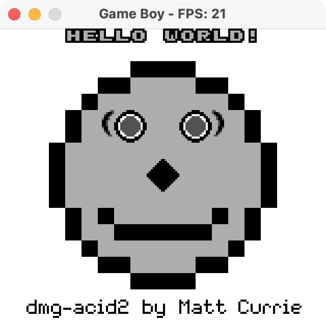
dmg-acid2 on my emulator
At this point, I started to run into some performance issues on the simulator. The performance of a Verilated module is orders of magnitude faster than it would be with other simulators, but you can only go so far trying to simulate a highly-parallel circuit. My eight-year-old laptop couldn’t quite keep up, and the simulator ran at only 50% speed (30 FPS) by the time I was done with my PPU.
After I had graphics mostly complete, I implemented the joypad input peripheral. For the simulator, I fed keyboard input from SDL to the appropriate joypad input signals in my module. This allowed me to start navigating through game menus and find even more graphical bugs. Pretty soon, I was even able to play some games. I started with Tetris and Dr. Mario, which were early titles for the Game Boy. They didn’t make use of all of the functionality of the system, so they were more likely to work with less of the emulator implemented.
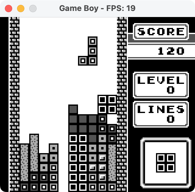
Waiting for a line piece
Implementing sound
Theoretically, I could have implemented sound before (or at the same time) as graphics. In practice, it’s helpful to be able to see what’s going on in the game and navigate menus. It’s also easier to debug what you see than what you hear, so sound can be kind of frustrating. A lot of hobbyists who implement emulators stop before implementing sound. In fact, for my first NES emulator, I didn’t implement any sound at all.
On the Game Boy, sound is produced by a component called the Audio Processing Unit (APU). If the PPU is a big state machine, the APU is best described as a bunch of interconnected counters. There are four separate audio channels that are all mixed together: two square wave channels, one arbitrary waveform (using “wave RAM”), and one “noise” channel. Again, for a detailed description, read Rodrigo Copetti’s article.
At this point, the performance issues of the simulator became very annoying. My framerate dropped to about 15 FPS. The human sensory system is much more sensitive to laggy/stuttering audio than video, and it became very hard to determine if my output was correct.
Stuttering audio in Metroid II
I ended up dealing with this by writing audio samples to a file as the simulator ran, and then playing them back afterwards at full speed.
Getting it running on the FPGA
Up until this point, I had been doing all of my development on the simulator. Once I had graphics and audio mostly working, I decided to work on getting my design built for and running on my FPGA.
I had already played around with Vivado (the Xilinx IDE) when I first got my Pynq-Z2 board. The GUI isn’t great, but fortunately all of Vivado is scriptable with Tcl and runnable via a CLI. I found a neat project called FuseSoC, an HDL build manager that abstracts over the vendor-specific build tools, so I wouldn’t have to interact with Vivado as much.
I set up FuseSoC to take care of invoking sbt (Scala Build Tool) to compile and run my Chisel/Scala code and produce Verilog, then pass that Verilog to Vivado to produce a bitstream for the specific Zynq chip on the Pynq-Z2. In addition to the generated Verilog source, Vivado also takes in a “Xilinx Design Constraints” (.xdc) file, a Tcl script that tells Vivado how the physical pins on the FPGA are to be configured. The Pynq-Z2 came with a base .xdc file that I customized to my needs.
After I got a basic LED blinker working (the hardware equivalent of a “Hello, World!” program), I moved on to trying out my emulator. I didn’t bother to set up HDMI output, or cartridge input or anything like that. I configured the core to act like there was no cartridge plugged in, and output the Game Boy LCD signals to some physical pins that I could probe with a logic analyzer. After battling the tools for a little while, I got it working.
For this project, I upgraded to a Saleae Logic 8 logic analyzer. I like it a lot: it’s a really nice piece of hardware, with some polished software to go along with it. My only complaint is that it still has a micro-USB port, rather than USB-C. The Logic 8 isn’t cheap, but Saleae offers discounts to students and hobbyists. I’d definitely recommend owning a logic analyzer, and the Saleae is a good choice if it’s within your budget. Otherwise, there are some really cheap logic analyzers you can get on Amazon/eBay/AliExpress, which are better than having nothing.
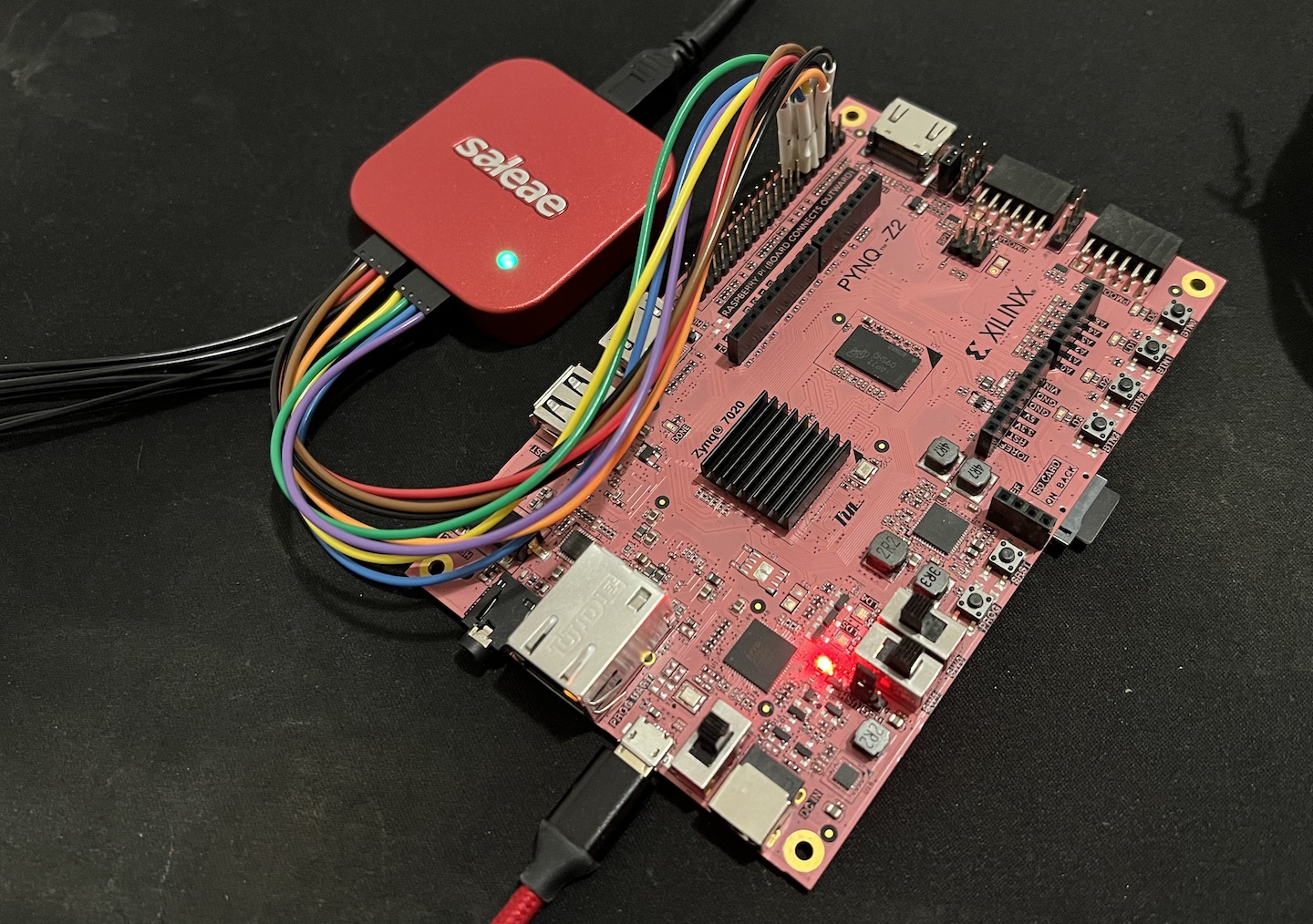
Saleae Logic 8 connected to the Pynq-Z2
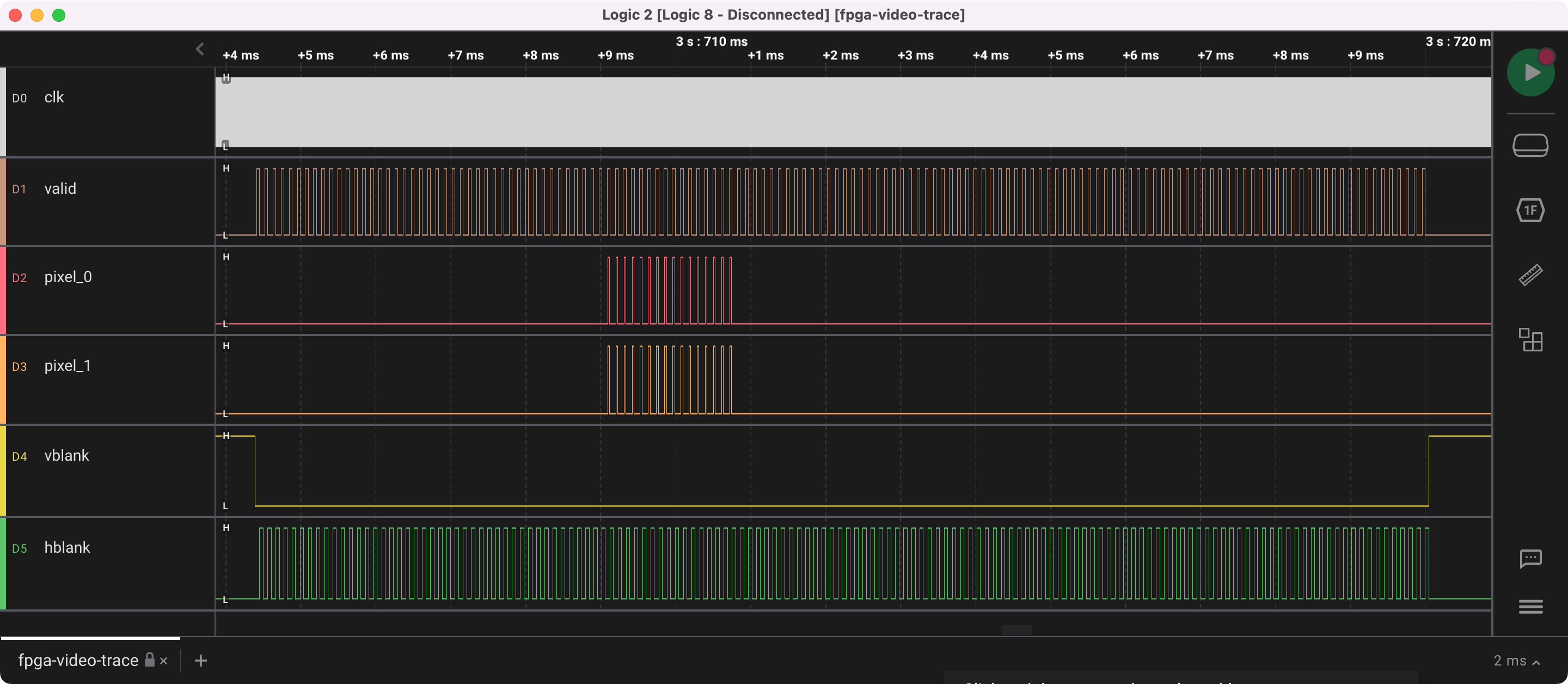
Trace showing one frame of video signals
I wrote a quick program to interpret the video signals from the logic analyzer and produce graphical output. Separately, I did a similar trick with the logic analyzer to get audio, so I could hear the classic Game Boy “di-ding!” sound. This led to the very first output from my emulator running on an actual FPGA. I knew the core of my emulator worked because I had been testing it with the simulator, but seeing actual output from a physical FPGA gave me a lot of satisfaction and the motivation I needed to keep working on the project.
Rendered audio and video signals from the FPGA, captured with logic analyzer
What you see above is what a Game Boy shows without any cartridge plugged in. The Nintendo logo normally displayed is actually read from the cartridge, and if there’s no cartridge, the logo is read as all 1s, which shows up as a block square.
The Game Boy was designed this way for legal reasons, to discourage unlicensed games. The boot ROM doesn’t start the game unless the Nintendo logo is correct, so an unlicensed game would have to violate Nintendo’s logo trademark. In practice, this doesn’t actually carry any legal weight in the United States, due to the decision in Sega v. Accolade, but it’s an interesting idea.
HDMI output from the FPGA
The next step was getting HDMI output from the FPGA, so that I could get real-time video and audio output from my emulator.
Some FPGA development boards have a dedicated HDMI transmitter chip, such as the ADV7513. The Pynq-Z2, however, directly connects its 2 HDMI ports to the FPGA, so it’s up to the FPGA to generate the HDMI signal.
HDMI is actually a proprietary standard, and you’re supposed to pay a fairly hefty licensing fee to use it. Fortunately, if you only need video (no audio), HDMI is fully backwards compatible with DVI. DVI doesn’t require licensing fees, and there are a number of free implementations for FPGAs. However, since I audio output, I needed to actually use a full HDMI implementation.
Fortunately, I found Sameer Puri’s open-source SystemVerilog implementation of HDMI. It was pretty easy to get working with a simple test pattern and tone.
Once I was confident that the HDMI output worked on my Pynq-Z2, I combined the HDMI module with my emulator module and got the first real-time audio and video output.
First HDMI output from emulator
The video output is repeated across the whole screen because the minimum HDMI output resolution is 640x480, and the Game Boy display is 160x144. The top-level module of my emulator writes the PPU’s video signals into a framebuffer, and in parallel, the HDMI module generates the output signal by reading from the framebuffer. For this initial demo, it was just a little bit simpler to tile the framebuffer rather than center it.
Using real cartridges with the FPGA
Falling black rectangles are cool and all, but I wanted to play actual game cartridges.
Towards the end of 2022, in anticipation of this project, I designed an adapter PCB that plugs into the top of the Pynq-Z2 and connects it to a cartridge slot.
A Game Boy cartridge (or, as Nintendo calls it, a Game Pak) has 32 pins:
- 2 power pins (+5 volts and ground)
- 16 address signals
- 8 bidirectional data signals
- 4 control signals: reset, read, write, chip-select (between ROM and battery-backed RAM)
- 2 mostly-unused signals: 1 MHz clock, and an analog audio input
This leaves 28 meaningful data signals. Conveniently, the Pynq-Z2 has a Raspberry Pi-compatible 40-pin header, with exactly 28 pins connected directly to the FPGA.
I planned to support multiplayer games over the Game Link cable, so I also added a link port. This added three signals (serial clock, data in, data out), which I attached to other exposed FPGA GPIOs.
The Game Boy runs at 5V, and since most modern devices (including microcontrollers and FPGAs) support at most 3.3V I/O, I had to add logic level shifters. Although only the 8 data signals were bidirectional, I decided to use four auto-direction sensing TXS0108E level shifters.
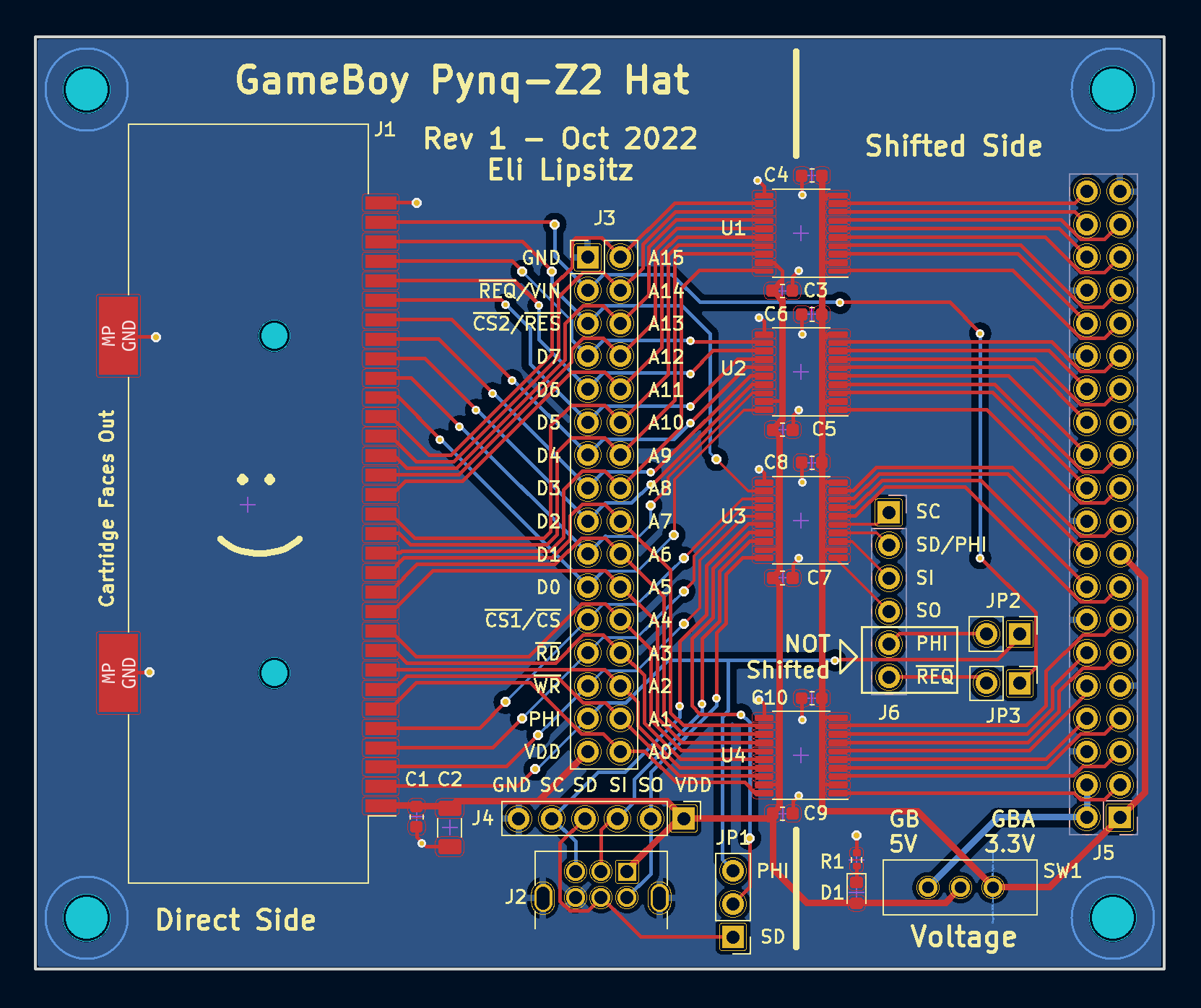
The adapter PCB in KiCad
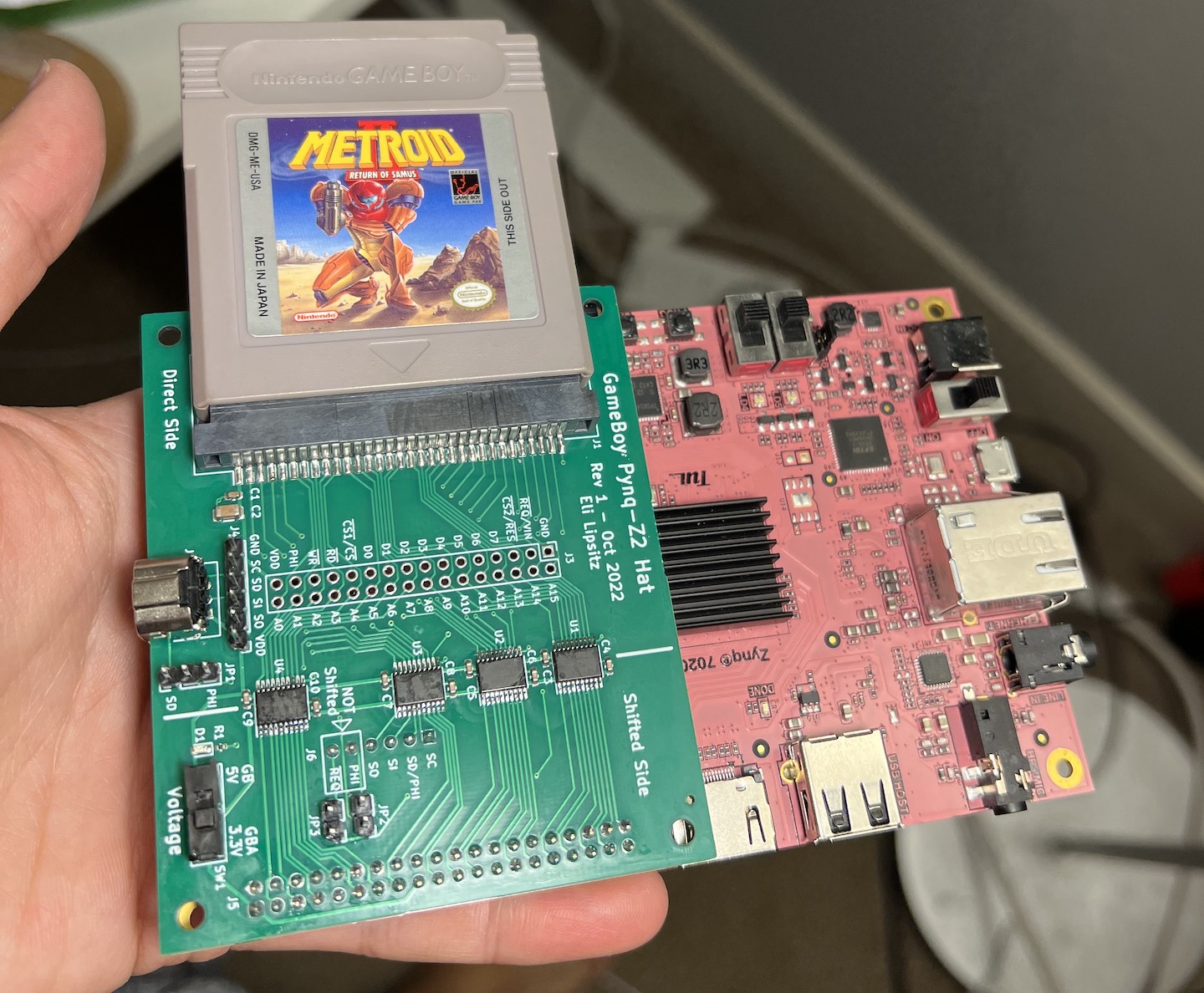
The assembled adapter board
As it turned out, auto-direction sensing level shifters weren’t the wisest decision, and the link cable didn’t work properly in the first revision. I made a second hardware revision that used a 74LVCH16T245, which used some additional FPGA pins to explicitly set the direction of each group of 8 pins for the cartridge, along with an individually controllable 74LVC1T45 level shifter for each link cable signal.
The assembled adapter board, revision 2
I designed these boards to be compatible with Game Boy Advance cartridges, in case I wanted to implement something with them in the future. GBA cartridges run at 3.3V, and switch the meaning of some of the pins. I added a switch on the board to switch the level shifter voltage supply between 5V and 3.3V.
After fixing a bad solder joint, the adapter board worked and I was able to run Metroid II from the cartridge.
Running Metroid II off of the cartridge
Input and connecting the Zynq Processing System
The next step was to get input working. I intended to connect an Xbox One controller to the Pynq-Z2 over USB, then have a program running on the Linux side listen for controller inputs and transmit them to the FPGA.
Up until this point, I was using the FPGA part of the Zynq chip (“PL”) directly. I used openFPGALoader to load the bitstream onto the FPGA over JTAG without using the ARM cores (“PS”) at all. If I wanted to do any PS/PL communication at all, I’d need to start building my bitstream with some additional PS configuration. After a lot of struggling, I came to the conclusion that this required using the Vivado GUI.
Vivado isn’t actually a terrible program, considering how much it does, but the interface is a litle bit janky. It didn’t help that I was running it in a Linux virtual machine on macOS.
With Vivado, you more-or-less need to use their graphical Block Design Editor to link together different pieces of IP (intellectual property, the chip design equivalent of a software library).
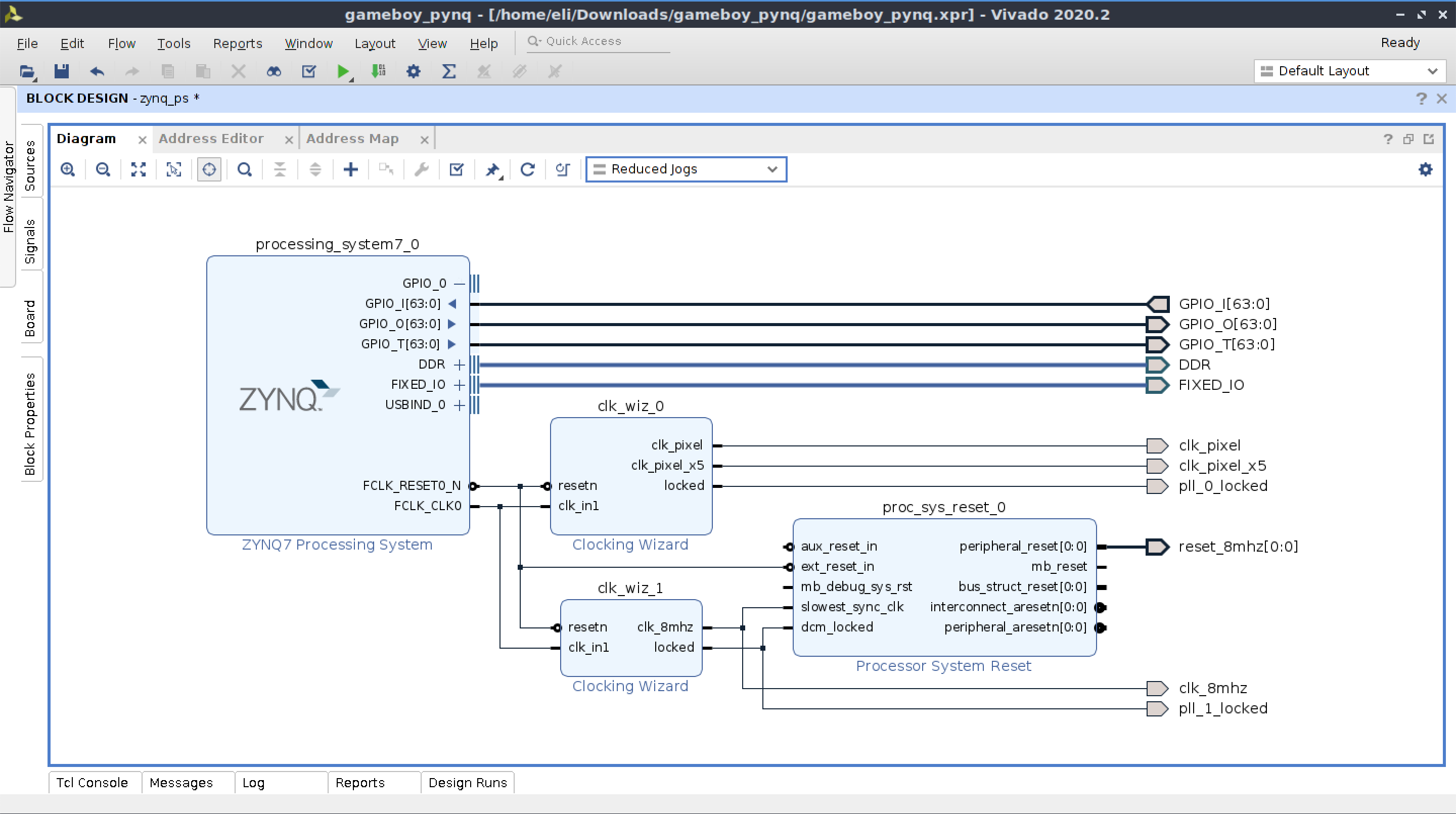
Block design in Vivado GUI
The key piece is the “ZYNQ7 Processing System” block. I configured some clocks through the Clocking Wizard, and enabled the PS GPIO signals connected to the PL. This is the simplest PS/PL interface offered: a set of 64 digital signals between the PS and PL. I used eight of these, one for each of the buttons on the Game Boy.
As a software engineer, I greatly prefer text-based configuration. However, one interesting thing about the Vivado GUI is that it’s essentially a wrapper around Tcl commands. As you click around in Vivado, it prints out the Tcl commands it’s running. I was able to export my block design as a Tcl file (containing the Tcl commands required to reproduce the design) and add that to my FuseSoC project as a source file.
Once I got my design building with the Tcl configuration for the PS, I needed a way to load it from Linux. JTAG was no longer sufficient, since the PS needed to be configured and running as well. Fortunately, the Pynq project that the Pynq-Z2 board was designed for made this straightforward. Pynq is essentially a set of Python libraries that make it easy to write software that runs on the PS and interfaces with the PL. Loading the design (an “overlay”, in Pynq terminology) was as simple as:
from pynq import Overlay
overlay = Overlay("gameboy.bit")
In addition to the bitstream (gameboy.bit), this required another artifact from the Vivado/FuseSoC build, the .hwh (“hardware handoff”) file for the build, which describes how clocks and certain PS/PL interfaces are configured.
Linux has support for Xbox controllers using the in-tree driver xpad. The Pynq-Z2 distribution of Linux didn’t include xpad, but after a lot of trial and error, I was able to build the driver using the Pynq Linux kernel headers and load it as a kernel module. I extended my Python loader script to listen for controller events (using the xbox360controller Python library) and set the GPIO outputs to the FPGA.
With input working, the main goal of the project was complete! I could now play physical Game Boy cartridges using my FPGA emulator.
Playing Metroid II with an Xbox controller
Emulating cartridges
As I stated in my project goals, I also wanted the ability to play games on the FPGA without a physical cartridge, to play homebrew and ROM dumps.
I mentioned previously that the Game Boy has a 16-bit address space, mapping 64 KiB of memory. Of this, 32 KiB addresses the cartridge. However, very few games actually fit into 32 KiB. Pokemon Red, for example, is 1024 KiB. Game Boy cartridges handle this by using Memory Bank Controller (MBC, or “mapper”) chips to bank switch different parts of the ROM into the limited address space. Emulating a cartridge thus also involves emulating MBCs. Fortunately, there are only a few common MBCs, and the mapping logic is pretty simple.
I planned to have the Linux side load ROM files into DRAM. The FPGA would emulate the mapping logic, translating the cartridge access signals from the core of the emulator into DRAM accesses.
This actually ended up being fairly complicated to implement. The Pynq-Z2 has 512 MiB of DRAM connected to a DRAM controller in the SoC, rather than directly connected to the FPGA. Both the PL and PS can access this through the central interconnect.
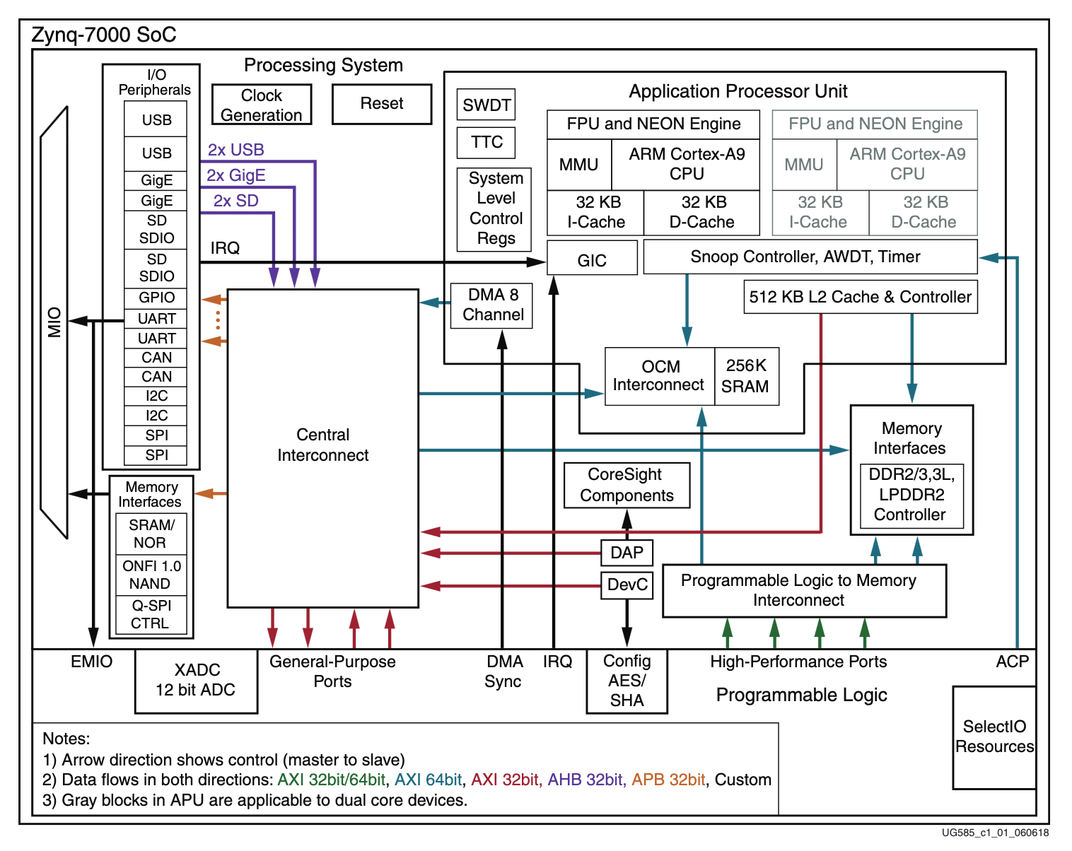
Zync SoC block diagram
The FPGA accesses this interconnect through an AXI bus. A program running on the PS needs to allocate a buffer in contiguous physical memory, load the ROM file into this buffer, and then pass the address of the buffer to the FPGA so that it can freely access the ROM as needed. The PS/PL GPIO is only suitable for simple control signals, like interrupts or the game controller inputs. For structured configuration data, the PL can expose an AXI interface that gets memory-mapped into the PS’s address space. Then, a program running on the PS can simply write to or read from certain memory locations to communicate information (like buffer physical addresses) to the FPGA.
To summarize, I needed to implement both an AXI target (to provide a control channel), and an AXI initiator (so that the FPGA could read the game ROM). This wasn’t actually too difficult because I didn’t need to support any fancy features such as pipelining or burst transactions for either the target or initiator. ZipCPU’s blog (1), (2) was a helpful resource.
I extended the Vivado block design from before to expose the AXI signals, and convert the AXI3 signals from the PS into the AXI4-Lite signals that I supported in the PL.
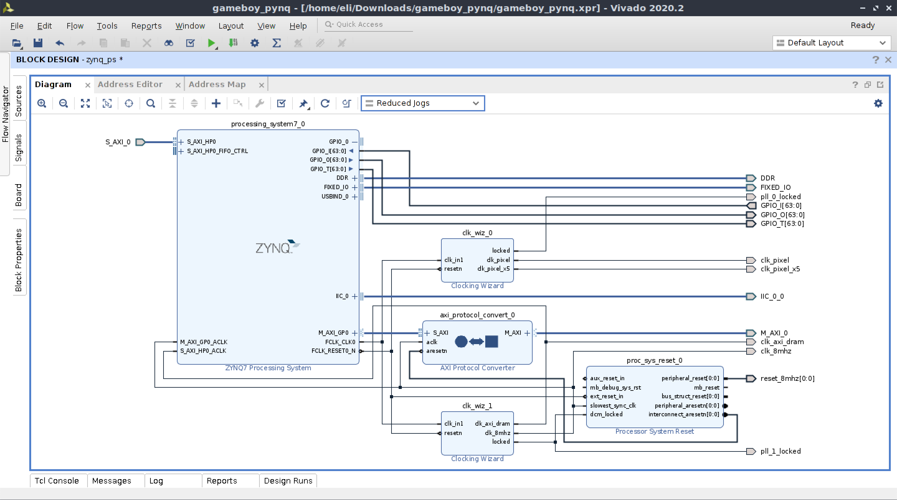
Block design in Vivado GUI with AXI connections
Once I had the infrastructure in place to support the AXI target on the FPGA side, it was easy to add more memory-mapped registers. I added registers for the PS to pause and reset the Game Boy, read the internal state of the CPU (for debugging), and read statistics.
Eventually, I had the ability to run arbitrary ROMs on my FPGA. I used a Python script running on Linux on the PS to load the bitstream onto the FPGA, allocate a buffer for the ROM file, and configure the FPGA with the buffer address.
Tetris running from an emulated cartridge
Since the DRAM controller was part of the SoC and out of my control, random access latency was unpredictable. Almost all memory accesses would complete within the 1 microsecond deadline, but some would occasionally take longer. This lead to occasional cartridge read corruption, with some amusing effects:
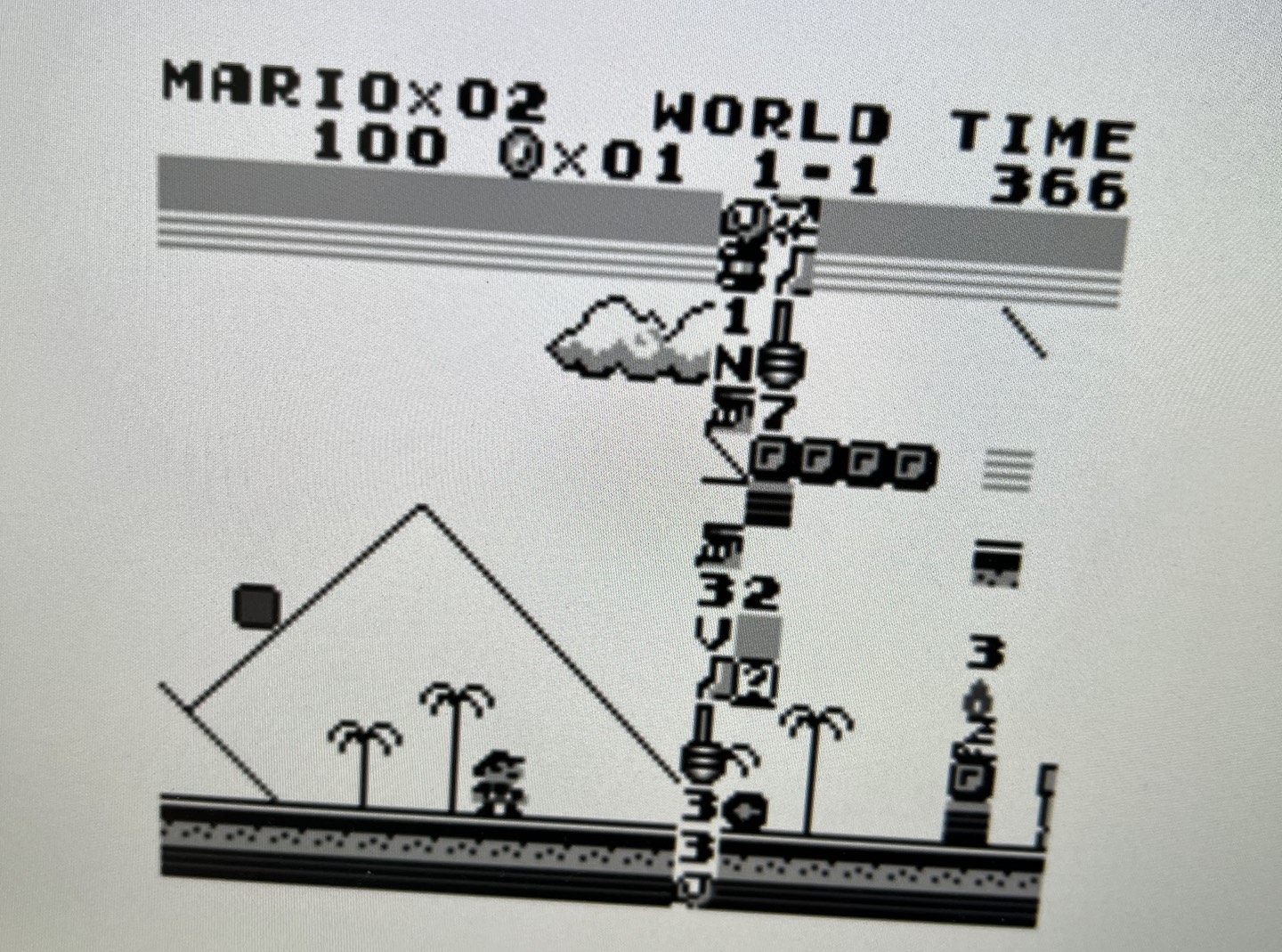
Mario facing an impassible wall of glitched tiles
The solution for this is pretty simple. If a cartridge read from DRAM takes longer than one Game Boy clock cycle, the emulator core is paused (i.e. not clocked) until the read has completed. I added a statistics register to see how often this was happening, and found that generally about 0.5% of the total emulator cycles were stall cycles. That is, games ran approximately 0.5% slower than hardware, which was imperceptible.
Game Boy cartridges that support persistent save files bundled a small amount of RAM in the cartridge, kept powered by a coin cell battery when not in use. I extended the cartridge emulation to support this: in addition to a ROM buffer, the Linux side also allocated a save RAM buffer. I added write support to the AXI initiator on the FPGA. When the game writes to cartridge RAM, the emulator writes to the shared RAM buffer. Then, I made the PS persist this to nonvolatile storage (and load from storage when loading a game).
At this point, I also implemented emulation for the real-time clock sometimes present in MBC3 cartridges. It wasn’t widely used, but it’s responsible for the day/night cycle in Pokemon Gold/Silver/Crystal. The time is persisted and restored based on the timekeeping of the PS. I used a helpful RTC test ROM to understand some of the edge cases of the chip.
Adding Game Boy Color support
The next part of the project was implementing support for Game Boy Color. The Game Boy Color (codenamed “CGB”, for “color Game Boy”) is extremely similar to the original Game Boy (codenamed “DMG”, for “dot-matrix game”), with a few added features:
- 15-bit color output
- 4x the work RAM, 2x the video RAM
- Optional double-speed mode (the CPU can run at 8 MHz instead of 4 MHz)
- Video RAM DMA support
- Other small miscellaneous improvements
Most of these weren’t too time consuming to implement. The color graphics are a straightforward extension of the original graphics. I implemented them in a day, with the help of the cgb-acid2 test suite.
The double-speed mode required the most work, because it required the ability to switch between 4 MHz and 8 MHz at runtime. In theory, I could have simply switched which clock I was feeding into the emulator module as needed, requiring essentially no code changes. However, due to the way FPGAs work internally, this is considered very bad practice. Clock signals require careful routing on dedicated fabric to avoid clock skew, and generally clocks generated from logic cannot use this fabric. Additionally, tooling can’t properly analyze the clock signal, leading to low quality analysis or even incorrect output.
Even if I were able to switch between the two clock speeds, different parts of the Game Boy Color run at different speeds. The CPU, timer, serial, and OAM DMA are affected by double-speed mode, but the APU and PPU always run at 4 MHz, and the video RAM DMA always runs at 8 MHz.
My solution to this was to use the 8 MHz clock everywhere, but generate different “enable” signals that allowed modules to skip clock cycles as needed, allowing them to run at 4 MHz speed.
After fixing a few bugs, I could now play Game Boy Color games:
Pokemon Gold running on the emulator
Fixing an audio bug on the Game Boy Color
After this, I used the emulated cartridge functionality to play a bunch of different games and demos to find emulation bugs. Some were simple to fix, some were amusing, some were frustrating, but one in particular was really interesting.
When I played The Legend of Zelda: Link’s Awakening DX, an updated version of the Game Boy classic with improvements for the Game Boy Color, I noticed that the audio in the opening sounded… very wrong.
Correct Link’s Awakening audio
Buggy Link’s Awakening audio
Interestingly, despite the fact that the DX edition of the game was released for the Game Boy Color, it can still be played on the original Game Boy. When I configured my emulator to act as a Game Boy, the audio sounded perfectly fine. And when I played the game on the Verilator-simulated version of my emulator, there were no audio glitches either.
I decided to record audio of the broken and working versions, and look at the waveforms side-by-side to see if I could tell what sort of audio distortion was happening. Once I recorded them, I didn’t even have to look at the waveforms before I noticed a very obvious discrepancy: the CGB recording of the opening cutscene was 10% longer than the DMG recording.
I immediately had a hunch about what was going on, and I checked the stats registers to confirm: the CGB version was stalling on DRAM access for more than 10% of the total cycles, compared to less than 0.5% for the DMG version. DRAM is optimized for linear burst accesses, rather than the random access of single bytes at a time required to emulate a Game Boy cartridge. The performance was sufficient for the original Game Boy, which did at most one memory access per 1 microsecond, but evidently it was not sufficient for the Game Boy Color in double-speed mode, which could do a memory access every 0.5 microseconds.
I believe that the reason the audio sounds terrible, rather than just pitched down, is because the speed decrease is non-uniform. Some DRAM access patterns likely took longer than others, or activity on the ARM cores caused intermittent contention. The non-uniform speed changes lead to a non-uniform pitch change, causing some sort of irregular, harsh vibrato.
The solution, of course, is caching. CPUs have had caches for decades to address this exact problem: large memories are slow, much slower than the CPUs they’re connected to. Before I spent time implementing a complicated cache, I decided to run some simulations. I augmented the simulator to record cartridge accesses so that I could measure the hit rates of different types and sizes of caches.
Since I was accessing DRAM over a 64-bit AXI bus, I fixed the cache line size to 64 bits (8 bytes). With a super simple single-entry cache, the hit rate was already at 91%. Increasing it to two entries (direct mapped), the hit rate went up to 95%. Increasing the size further improved the hit rate, but with quickly diminishing returns. Increasing the associativity helped a little bit too.
I decided to stick with a direct mapped cache. Implementing a set-associative cache would have greatly increased the implementation complexity, and a direct mapped cache of even moderate size was more than sufficient. I decided to use a 512 entry cache. This was beyond the point of diminishing returns, but Xilinx Series 7 FPGAs group block RAM into chunks of 18 or 36 KiB, so there was no reason to use anything less than a full block.
After implementing the cache, the stall rate was down to an acceptable level and the glitchy audio was fixed.
Adding an on-screen menu
At this point, to play a game, you’d have to connect to the Pynq-Z2 Linux console (or SSH in) and run the script with the path to the ROM file. I wanted to add a more user-friendly way to browse and run games, via an on-screen menu navigable with the controller.
I considered implementing the menu as a custom Game Boy ROM that used special memory addresses to communicate with the PS script. However, I also wanted to be able to have an in-game overlay menu, so I opted instead to implement the interface entirely on the PS side. Since the FPGA was still responsible for HDMI output, I’d need some way of sending rendered frames over to be displayed.
At first, I experimented with setting individual framebuffer pixels from the PS through the memory-mapped configuration registers, because it was simple to implement. However, doing this as a bunch of individual (non-burst) writes from Python was far too slow, with a full-screen refresh taking on the order of half a second. Instead, I ended up having the FPGA quickly pull the rendered frame (again using the AXI initiator) from a shared memory buffer (when told to via a configuration register). This was significantly faster, with imperceptible transfer time.
I created a super simple UI framework, rendered in Python with the Pillow library. Through the menu, you can play the connected cartridge, or choose from a list of ROM files. In the middle of a game, you can bring up the menu again and reset the emulator or go back to the main menu to select another game.
Navigating the on-screen menu
I called the project “Game Bub”, a play on “Game Boy”, and created a logo to match.

Dictionary definition of ‘bub’
I configured Linux to run the Python program on boot, so that the emulator could be used without needing to be controlled by another computer.
Implementing link cable functionality
The last thing to do was to implement proper link cable functionality, to allow my emulator to communicate with a real, physical Game Boy. I had previously attempted to get this working back when I had first gotten the emulator running on the FPGA, but ran into issues with the first version of my adapter board. With the second version of my adapter PCB, I fixed these issues and could try again.
Weird stuff happens when the link cable doesn’t work properly
The link cable functionality is actually very simple. The Game Boy uses a simple serial protocol, essentially SPI. There are three signals involved: clock, data in, and data out. One device generates the clock signal, and the other receives it. Each device has an 8-bit data register, and each clock edge, one bit gets shifted out to the other device, and one bit gets shifted in. All multiplayer game protocols (e.g. Pokemon trading, 2 player Tetris) are built on top of these simple byte-wise transfers.
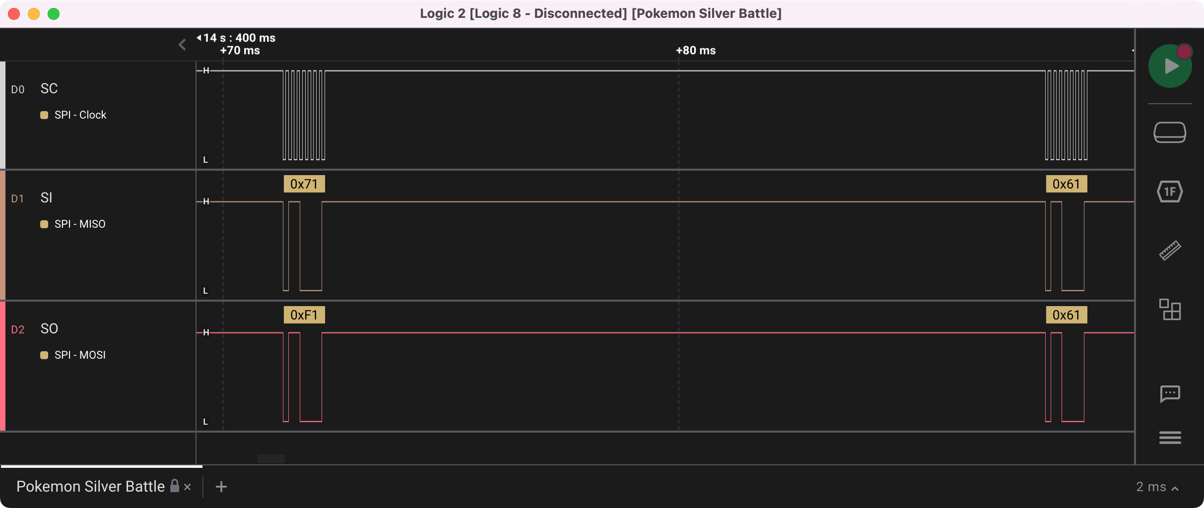
Link cable communications during a Pokemon battle
I designed my PCB to break out the link cable signals so that I could observe the flow of data using my logic analyzer. There’s no way to observe the serial connection otherwise, so the logic analyzer was super useful. Despite the simplicity of the serial protocol, I had a few off-by-one errors that prevented proper communication. Eventually I resolved these, and I could do a multiplayer Pokemon battle:
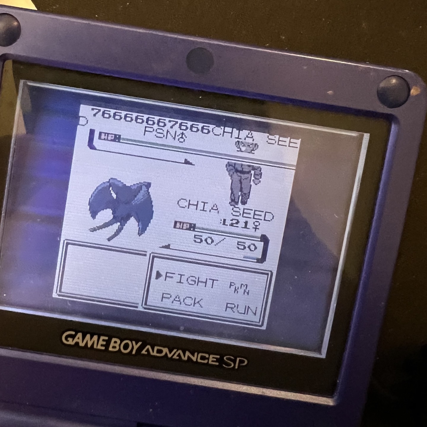
A Pokemon battle between the emulator and a real Game Boy Advance
Conclusion
And with that, the project was complete! In a few months, I was able to complete all of my goals: I created a fully functional FPGA-based Game Boy emulator, runnable on a real, physical FPGA, with HDMI output and game controller input, with the ability to play both physical cartridges and virtual ROMs, as well as interface with other Game Boy devices over the game link cable.
I also learned quite a bit about FPGAs, and I had a lot of fun (and frustration).
I debugged countless bugs not mentioned here. Many of them were purely emulation bugs: the road to building an emulator is filled with debugging edge cases. However, a lot of them related to the FPGA: with no prior experience, I struggled a lot.
As it turned out, my mental model of an FPGA that runs Verilog perfectly wasn’t quite accurate. In particular, timing is a huge part of the design process. The FPGA toolchain needs to be able to analyze the design to ensure it meets timing requirements and analyze clocks and other resource usage. In particular, clock domain crossing, which happens any time you use a signal generated from one clock with logic or flip-flops controlled by another clock, adds a significant amount of additional complexity. Even worse, timing bugs tend to be non-deterministic, and the physical nature of FPGAs already makes them difficult to debug.
Although this project may have been a little ambitious for someone with so little FPGA experience, I definitely had a lot more motivation working on a real, interesting project.
I intend to keep working on this project in the future. There are all sorts of additional features I could add: save states, screenshots or recordings, better debuggability, or even rewind. Or, perhaps I’ll move on to implementing more complex consoles, like the Game Boy Advance.
Acknowledgements
- All of the Pan Docs contributors
- Joonas Javanainen (gekkio) for his Game Boy research and documentation
- Everyone in
#gbon the Emulation Development Discord - Rodrigo Copetti for his excellent “Architecture of Consoles” series
- blargg, for their Game Boy test ROMs
- Matt Currie for the
dmg-acid2andcgb-acid2test ROMs. - Martin Schoeberl, for his free Digital Design with Chisel book.
- Sameer Puri for his open-source HDMI transmitter
- Dan Gisselquist for helpful FPGA articles
- I used numerous open-source projects, including Chisel, FuseSoC, Pynq, Verilator, and KiCad.
And many other people who wrote blog posts, articles, and other resources about the Game Boy, FPGAs, and Vivado.