I built a device that allows a pinball machine from 1984 to automatically upload scores to the internet. The device taps into the machine’s memory bus and monitors the game state, uploading scores after each game.
You can find all of the code and design files on my GitHub.
Background
Growing up, my family owned an old pinball machine, a 1974 Williams Strato-Flite. Strato-Flite is an electromechanical (EM) pinball machine. In an EM machine, the game logic, scoring, and everything else is implemented through the use of relays, motors, and switches. As a result, Strato-Flite is quite primitive by modern standards. Even so, it’s impressive what the engineers at Williams were able to do with these constraints.
I’m really fortunate to have grown up with a Strato-Flite machine. Although pinball peaked in popularity long before I was born, I gained an appreciation for the game.

Me playing Strato-Flite (a while ago)
Some time later, my family acquired another pinball machine, a 1984 Williams Laser Cue. In the ten years between the two machines, there were immense advancements in the world of pinball, enabled by integrated circuits and microprocessors.
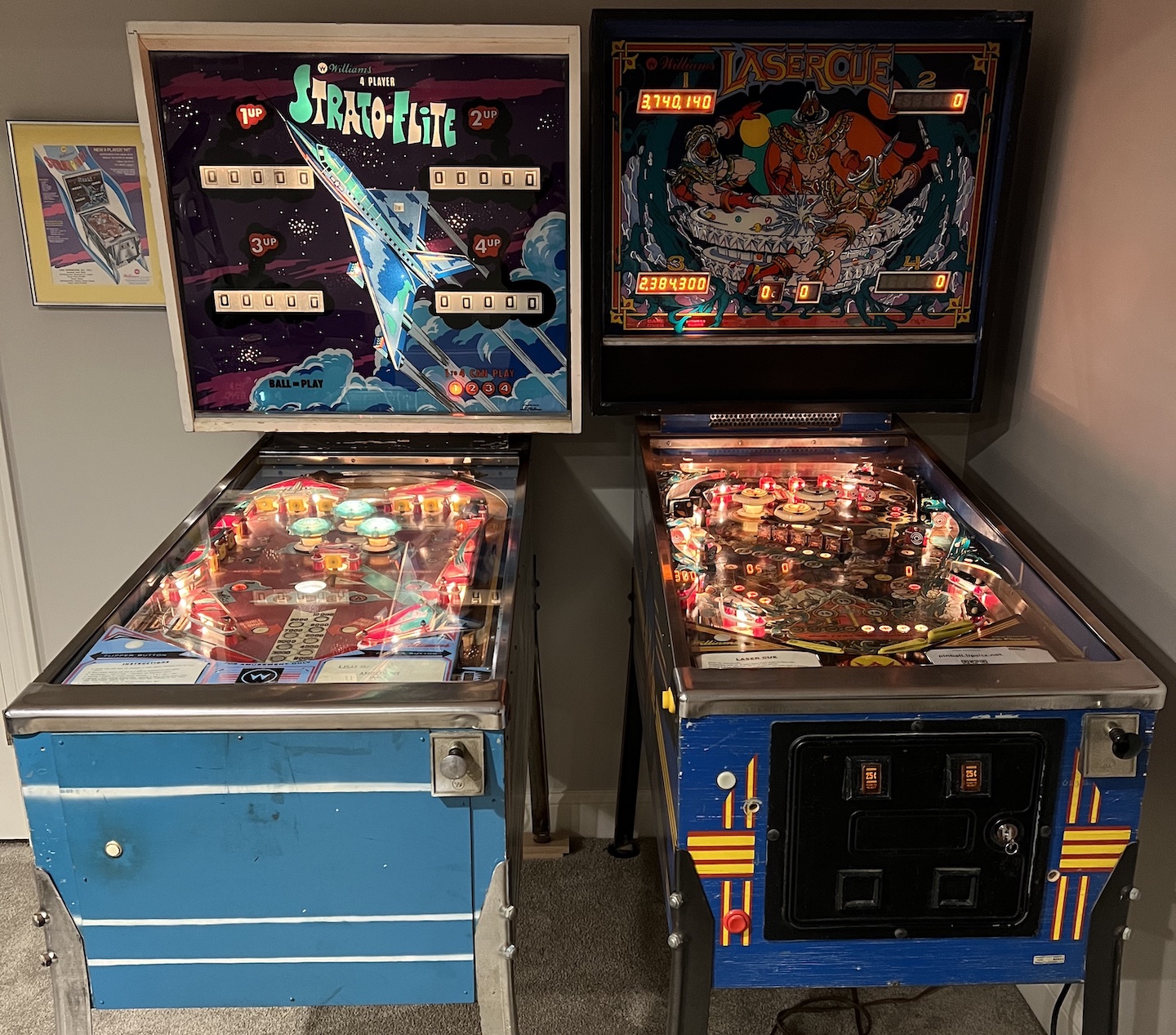
Strato-Flite and Laser Cue
I was impressed by the new machine: it had flashing lights, a simple soundtrack, sound effects, and a digital score display. Additionally, the gameplay was more complex and engaging. The overall objective of the game is to hit a series of switches in a particular order to earn “pool balls”. Some switches increase score multipliers and bonuses, or provide additional ways to earn “pool balls” and extra plays. Notably, unlike Strato-Flite, Laser Cue maintains each player’s playfield throughout the whole game. It’s a lot more fun to be able to build up your progress over the course of the game.
Pinball machines with integrated circuits are referred to as “solid state” machines. Those with microprocessors generally have another interesting feature: high scores. With Strato-Flite, you’d have to write down your best scores if you wanted to brag. Laser Cue, however, flashes the four highest scores whenever a game isn’t being played.

Laser Cue high score display
The idea
It was cool to see the top four scores, but it would be even cooler to be able to view all of the scores, when the game was played, and who earned the score. Ideally, I wanted the scores to be displayed on a website, automatically uploaded by the machine. I set out to build a device that would add internet connectivity to Laser Cue.
I’m not the first person to think of doing this to a pinball machine. There’s even a commercial off-the-shelf product for this: Scorbitron. Scorbitron is an impressive-looking piece of hardware, but it requires a $300 probe and a monthly subscription. Plus, what’s the fun of buying something when you could spend dozens of hours building it yourself? And perhaps most importantly, it doesn’t actually support Laser Cue.
I set a couple of goals for this project:
- Scores should be uploaded automatically by the machine.
- It should be reliable. Even if the internet connection goes down, or the game gets shut off before scores can upload, no scores should be lost.
- The machine should remain externally unchanged.
- Under no circumstances should this damage the machine. After all, it’s survived nearly 40 years without any major issues, a “nice to have” feature like this one shouldn’t be the end of it.
There was one more constraint: I don’t live near the machine, so I’d have only occasional opportunities to test my device.
Laser Cue: hardware and software
Generally, a pinball manufacturer would engineer a common pinball platform, and then use it to build many different pinball games, each with their own theming and gameplay.
Laser Cue is a Williams System 7 game. The linked PinWiki article has a wealth of information about the system, and served as an important resource for this project. System 7 is driven primarily by a Motorola 6808 microprocessor, with the help of a few Motorola MC6821 Peripheral Interface Adapters (PIAs) to control the display, playfield lamps, solenoids, and switches. It has 1 KiB of RAM, up to 12 KiB of ROM, and 128 bytes of battery-backed CMOS RAM (for storing scores and bookkeeping information). The main board that holds the microprocessor, RAM, and ROM chips is referred to as the MPU board. The machine uses 5 V TTL logic, compared to the 3.3 V (or less!) CMOS logic used by most modern microcontrollers.
Pinball machines generally came with manuals and detailed schematics to help operators troubleshoot and repair their machines. The System 7 schematics are freely available, and pretty easy to understand with some basic knowledge of digital electronics. The ICs used in the machine have long since been discontinued, but the datasheets for the important ones are fortunately easy to find online.
The Motorola 6808 (datasheet) is an 8-bit microprocessor that runs at 1 MHz, with a 16-bit address bus and an 8-bit data bus. Like the rest of the logic ICs, it uses 5 V TTL logic.
All System 7 machines share a common operating system, called the Flipper ROM. It’s a pretty impressive piece of software: it occupies only 6 KiB of ROM, and implements a multithreaded virtual machine with facilities for keeping track of switches, solenoids, and lamps. Individual games (such as Laser Cue) have their own Game ROM that contains the logic for the specific game. The software side of the system is well documented by Jess Askey in his unofficial Williams Level 7 Programming Manual, and on GitHub.
Intercepting memory writes
From Jess Askey’s documentation, we can see that the 1 KiB of RAM is mapped at 0x0000 - 0x00FF and 0x1000 - 0x13FF (the low 256 bytes are mapped to two locations for compatibility reasons). The game has two 4-byte score buffers for each player (0x38 and 0x48 for player 1, 0x3C and 0x4C for player 2, etc.). The scores are stored as binary-coded decimal (BCD), where each 4-bit nibble represents one decimal digit of the score. The pairs of buffers are used for quickly swapping between two scores, to alternate between the previous game’s scores and the high scores after a game over. Other memory locations store the game over flag, the current player, the current ball, and other game information.
Since all of the data is stored in external RAM chips (the MC6808 has no internal RAM), my approach was straightforward: build a device that taps into the CPU’s memory bus and watches for writes to RAM. The device would monitor key memory locations (score buffers, game state), then wait for a game over event and upload the scores. Modern microcontrollers run far faster than 1 MHz, so I figured it would be possible to do this without too much trouble.
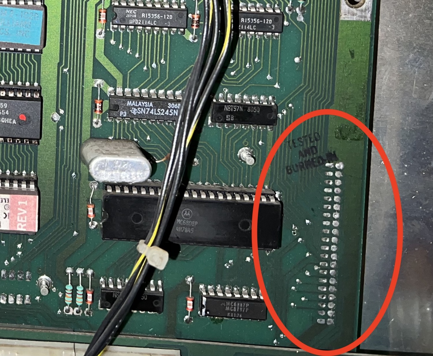
The 6808 is a 40-pin DIP IC, and it’s inserted into a socket on the MPU board, rather than being directly soldered into the PCB. My original idea was to create an interposer board that would plug into the CPU socket, containing another IC socket (that the actual 6808 would be plugged into), with wires to connect the memory bus to a WiFi-enabled microcontroller. I found a blog post from someone who did a similar thing, with a Z80 on a 1987 arcade game.
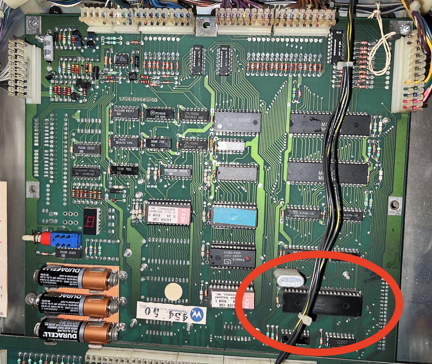
MPU board, highlighting the MC6808 microprocessor
This approach has the advantage of avoiding a permanent modification to the machine. The interposer board could be removed, and the CPU inserted back into the slot. I spent a significant amount of time researching different types of pin headers, trying to figure out which ones would fit most easily into the socket without damaging it. Unfortunately, the common square pin headers are a fair amount thicker than DIP IC pins. Although I wasn’t able to find any headers that mimicked IC pins, I found a couple of options that seemed thin enough.
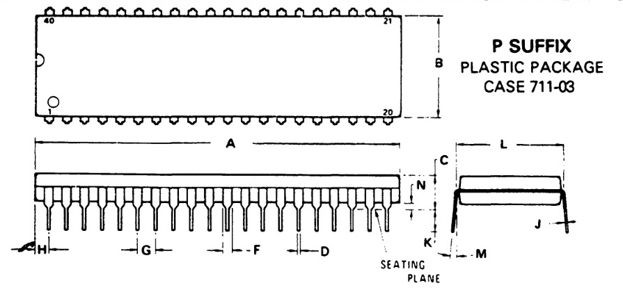
Physical diagram of the MC6808
However, when I decided to remove the 6808 from the machine to take a few more measurements, I found out that it took a large amount of force to remove. The MPU board is fairly large, and the board itself is thin and flimsy-feeling, so the circuit board was flexing an uncomfortable amount when I was trying to unseat the chip. I was worried that I would damage the machine, so I decided to stop and figure out a safer way to remove the chip.
During another read-through of the PinWiki page, I noticed that it said the System 7 MPU boards had an unpopulated 0.1 inch 2x20-pin connector, with pads that connected to all of the important signals on the board, including the entire memory bus. Presumably, Williams used this to test MPU boards during manufacturing or to perform diagnostics. I took another look at my machine’s MPU board and observed that the connector was present, as expected.
Unpopulated MPU test pads
Although using this connector would involve permanently modifying the board (to solder in some headers), it seemed like a more reliable and simpler way to tap into the memory bus. My device would just need a matching 2x20 pin connector, and then I’d have easy access to all of the relevant signals.
Decoding the address bus
I started by reaching for the Espressif ESP32, a powerful (dual 240 MHz Xtensa cores) and inexpensive microcontroller with built-in Wi-Fi. The ESP32 input pins are apparently 5V tolerant (apparently confirmed by the CEO of Espressif, albeit not listed in the datasheet). This meant I wouldn’t need to use any additional chips to shift the 5 V logic of the 6808 down to the 3.3 V logic of the microcontroller. However, I quickly spotted a problem: in order to decode the MC6808 memory bus, I’d need 27 inputs: 16 for the address bus, 8 for the data bus, one for the clock, one for the “valid memory address (VMA)” signal, and one for the “read/write” signal. On my 30-pin ESP32 dev board, there are only 25 GPIOs exposed. And of those exposed GPIOs, three of them have boot-time behavior that renders them unsuitable (e.g. they’re sampled at boot to configure the SoC, or they output a signal at boot, which could damage the pinball machine).
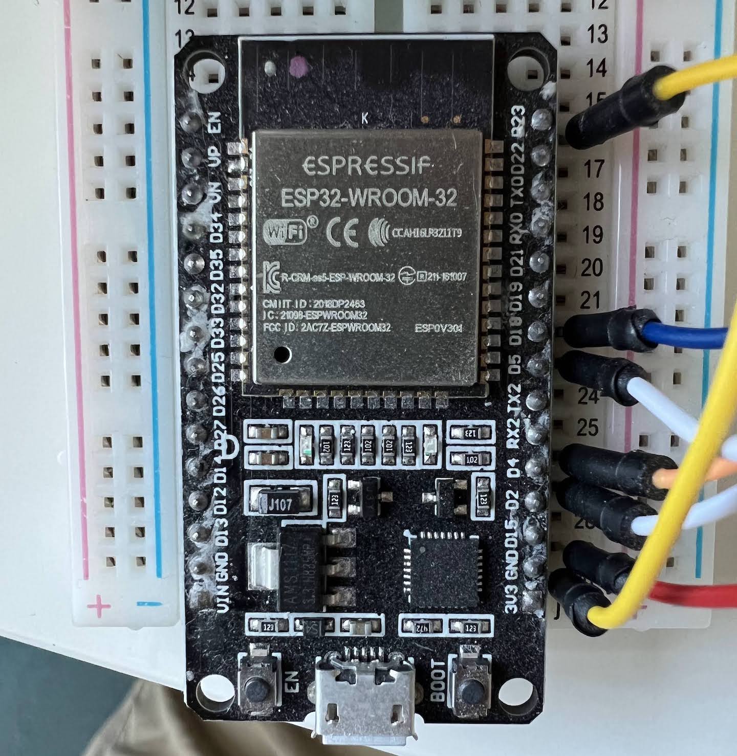
ESP32 dev board
I resolved this problem by realizing that since I only care about the 1 KiB RAM region, I didn’t actually need the microcontroller to decode the full address bus. As long as it could access the lower 10 bits, I could use external logic to decode the upper bits (and control signals) to determine if there was a valid write to the RAM regions. This substantially cut down on the number of inputs needed: 10 for the address bus, 8 for the data bus, one for the clock, and one for the decoded “valid write to the RAM region” signal, for a total of 20 inputs.
Next, I had to figure out how I’d do the address/control decode. My initial thought was to use discrete 74-series logic chips, which is what the System 7 MPU does. However, it would be pretty annoying to hand-wire them all up. I thought about using an FPGA, but that would be way overkill, plus modern FPGAs are not 5 V tolerant, don’t come in DIP packages, and FPGAs were nearly impossible to find (due to the chip shortage). A multitude of Google searches later, I found the Microchip ATF16V8B. The ATF16V8 is an electronically programmable logic chip with 250 gates (more than I need, but nothing ridiculous) and up to 18 I/O pins. Plus, it’s available as a DIP IC, it’s 5 V tolerant (but outputs 3.3 V signals), and it was readily available for cheap from sources like DigiKey and Mouser.
The ATF16V8 is kind of annoying to program, requiring an old Windows-only program called WinCUPL (I didn’t have much luck with the open-source alternatives), and an EEPROM programmer. I didn’t have an EEPROM programmer, and I didn’t feel like buying a TL866II Plus that I’d probably only use once. Instead, I found Afterburner, a programming device I could build myself with an Arduino. I probably should have just bought the TL866II Plus though. It was a pain to acquire the MT3608 voltage booster module that Afterburner used (and modify it to break out the IC’s “enable” pin), and build the thing on a breadboard. But it worked, so there’s that.
Programming the ATF16V8 with the Afterburner rig
I read the address decode logic off of the MPU schematic. After writing a short script to test my interpretation of the logic, I realized that something was off: the memory regions that my logic decoded to the RAM didn’t align with the memory map in the Programming Guide. After double and triple checking my logic, I realized that there must be an error in the schematic. I used a logic probe to test various connections on the board, and found out that an input to one of the gates was mislabeled as “A7”, when it should have been “A9”.
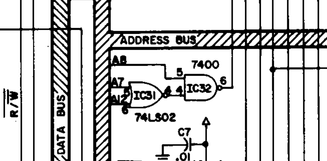
Pin 5 of IC31 is actually connected to A9
I probed some other connections to be extra sure, but I didn’t find any other errors. Satisfied the logic was correct, I wrote and compiled the ATF16V8 program with WinCUPL. In total, I used 7 inputs (A8, A9, A12, A13, A15, R/W, and VMA) and one output (“write enable”), with plenty of pins left unused on the chip.
Motorola 6808 bus timing
Next, I thought about what the ESP32 would do. I decided to dedicate an entire core to reading the memory bus and maintaining a 1 KiB shadow buffer that reflected the state of the RAM. Then I’d have the other core periodically check on addresses that I care about (reading scores and detecting game overs), as well as all of the other tasks, like Wi-Fi and uploading scores.
I was most concerned about the timing-sensitive code reading from the memory bus. To meet the 1 MHz clock, I had a budget of 1000 nanoseconds to detect each memory read. The ESP32 has two banks of GPIO, pins 0-31 in bank 1, and 32-39 in bank 2. Each bank can be read with a single 32-bit memory read that takes approximately 50 nanoseconds. Even though my inputs were spread across both banks and I had to do bit operations to extract the relevant signals, I clearly had plenty of time remaining in the budget.
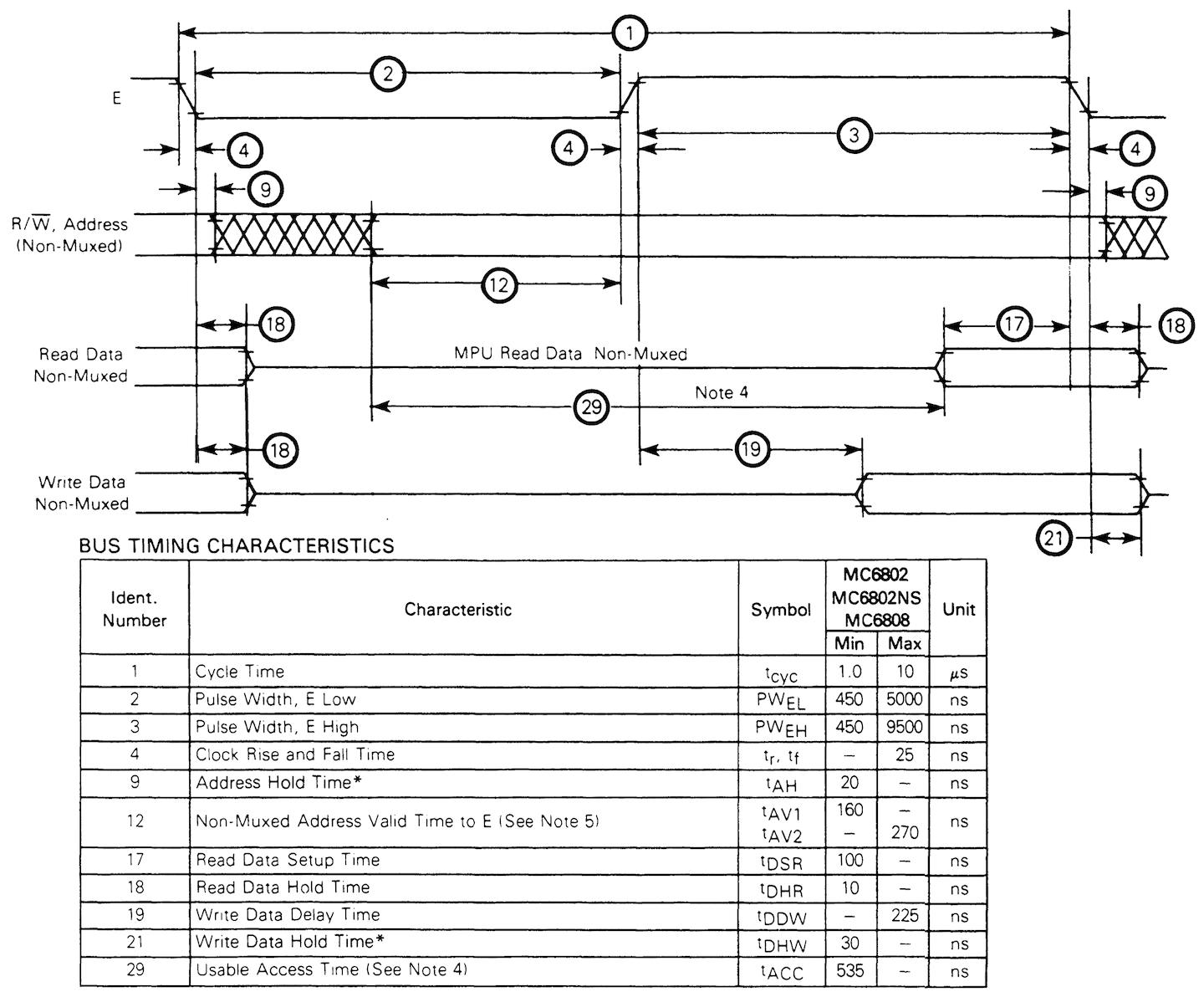
MC6808 bus timing diagram
The 6808 datasheet had a very helpful bus timing diagram, from which I derived a few key pieces of information:
- The address (and control) signals are valid at least 160 ns before the clock goes high.
- The address signal remains valid at least 20 nanoseconds after the clock goes low.
- The data (for a write) signal becomes valid at most 225 ns after the clock goes high. Based on the minimum clock pulse width of 450 ns, this means it’s valid for at least 225 ns before the clock goes low.
- The data signal remains valid for at least 30 ns after the clock goes low.
There’s plenty of time to read the address signal, but the timing is tight for the data signal. Since it’s only valid for 30 ns after the clock goes low, and a GPIO read takes 50 ns, I decided to continuously read the data signal, relying on the clock falling to know whether the read was actually valid. This leads to a simple algorithm, synchronized to the clock signal:
- Wait for the clock to go high.
- Check the “valid write” signal (from the ATF16V8). If it’s not valid, wait for the clock to go low and try again.
- Otherwise, snapshot the 10 address bits.
- Continuously snapshot the 8 data bits until the clock goes low, taking the last measurement before the clock went low.
- Apply the write to the internal buffer, and repeat.
Designing the circuit
Even though the ESP32 apparently had 5 V tolerant inputs, I decided to use 5 V to 3.3 V level shifters anyway. I was actually more concerned that the voltage levels would be too low. The 6808 datasheet said that the “Output High Voltage” was at least 2.4 V, and the ESP32 datasheet said that the “High-level input voltage” needed to be at least 75% of the supply voltage, or 2.48 V. This was cutting it pretty close, so I decided I’d rather be safe than sorry.
After triple-checking the voltage levels of the 6808 and the ESP32, I settled on the 74LVC245, a level shifter readily available as a DIP IC. Each chip has 8 I/O pairs, and I needed to level-shift 19 signals (10 address, 8 data, and 1 clock). Normally, this would mean I needed three level-shifter chips. However, I realized that I could repurpose the unused pins on the ATF16V8 to save a chip. The ATF16V8 has 18 I/O pins, but I was only using 7. I decided to pass it the clock signal and two of the address signals, using the programmable logic to output the signals level-shifted, but logically unchanged.
My original plan for this project was to solder the chips to a protoboard (example), and hand-wire all of the connections. I looked at custom PCB pricing though, and realized it would be as cheap, easier, and far cooler to design my own PCB.
I used the open-source electronic design software KiCad 6 to design my schematic and PCB. I was extremely impressed by the software. It was easy to use (after following a YouTube tutorial from Phil’s Lab), powerful, and highly polished. Overall, I had a great time designing my first PCB, and I’m excited to do it again some time in the future.
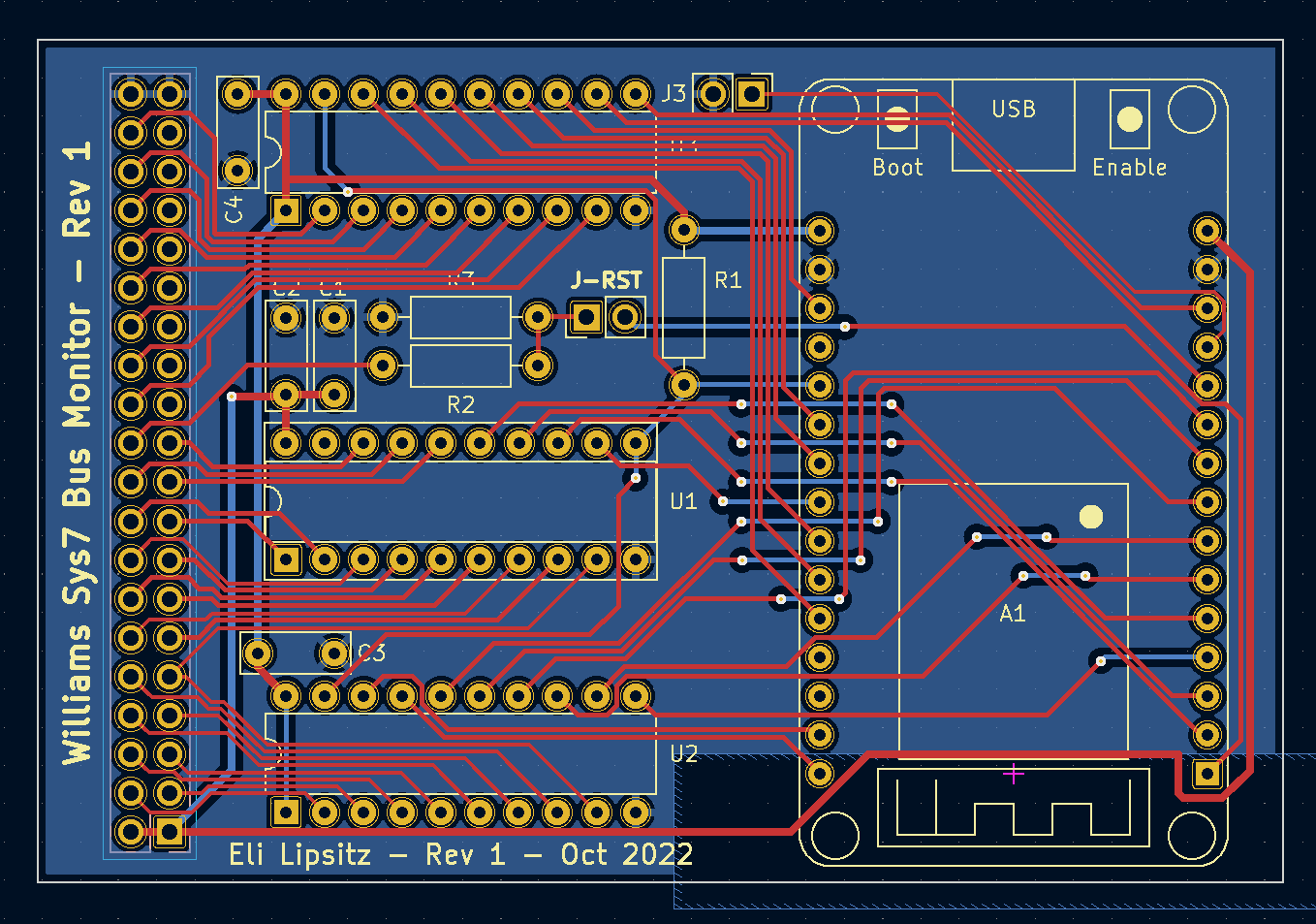
The completed PCB in KiCad
I ordered the PCB from JLCPCB, where it was about $3 plus a few dollars for shipping (I decided to spend an extra dollar to get it lead-free). While I was waiting for the PCB to arrive, I ordered the parts from Mouser. A couple weeks later, the PCBs arrived and I got to hold them in my hand, which was super cool.
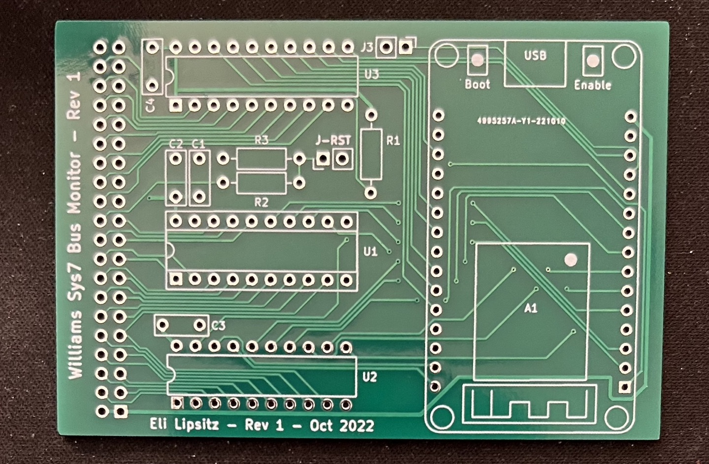
The manufactured PCB, in classic green
Testing the device
I soldered everything together with my Pinecil V2. It had been a while since I’d last soldered, so my first few joints were pretty bad. After a couple dozen, I got the hang of it and the rest went smoothly.
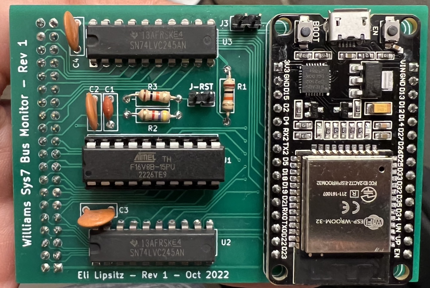
The assembled device
After admiring my handiwork, I started testing the device. I wouldn’t have access to the pinball machine for a few more weeks, so I had to simulate the memory bus somehow.
I had recently purchased a Raspberry Pi Pico, because I was intrigued by the Programmable I/O (PIO) of the RP2040. It excels at I/O with precise timing, so I figured it would do a good job simulating the specific timing characteristics of the 6808 memory bus.
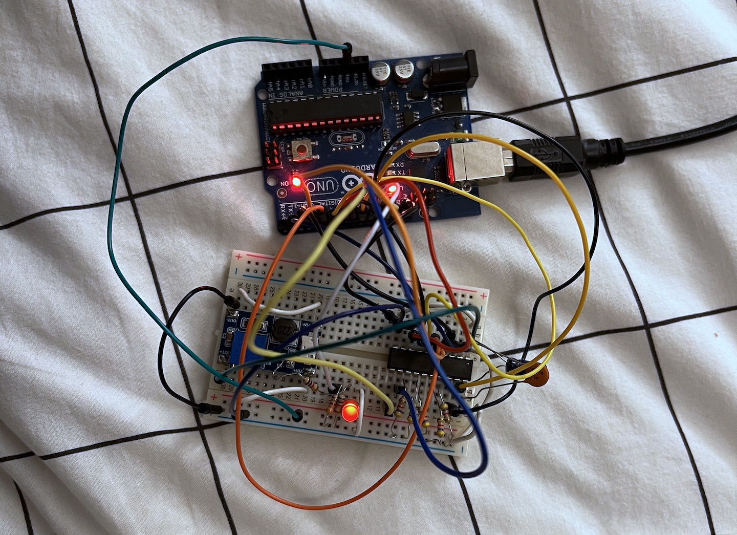
The test setup was simple: the Pico generated write signals at 1 MHz at a series of addresses and with a variety of values, to exercise all of the input pins. The PIO was carefully written to simulate the worst-case timing of the 6808 memory bus. The Pico did one million simulated writes, and the ESP32 counted how many it detected and a simple checksum of the data it received.
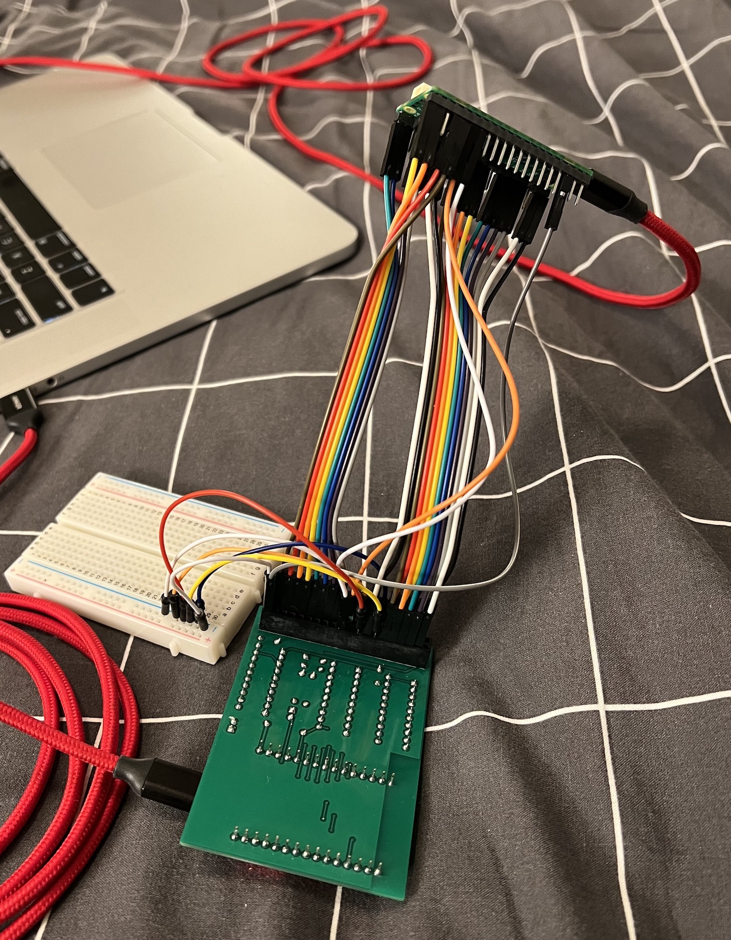
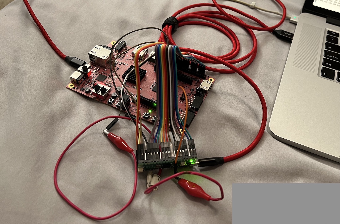
The test rig
I wrote the test and wired everything together, and it worked… sort of. It was wired up correctly: the ESP32 detected a write to every address and received every one of the possible 256 data values, but the final count was not one million. It was actually about 10k off, meaning about 1% of writes were not properly detected.
I wasn’t okay with missing even a single write — after all, I wanted this to be reliable, and what if that missing write carried an important state change? And given the theoretical timing, there’s no reason the hardware would miss any of the writes.
I spent a while debugging over the next few days. I tried to make sure that the Espressif SDK wasn’t scheduling any work on the second core, with a high priority FreeRTOS task. I attempted to disable interrupts on the second core, but that isn’t really supported by the SDK (and I found a few forum posts about it: [1] [2]). My most successful attempt came when I initialized the second core myself, running FreeRTOS in single-core mode (following someone’s guide). It required some modifications to the Espressif SDK, but even then, I was still missing tens of writes every second.
I came to the unfortunate conclusion that the ESP32 simply wouldn’t work for me. I still don’t understand exactly what the problem was (bus contention? secret interrupts? clock jitter?), but the chip just doesn’t seem well suited for something like this. I read through the ESP32 Technical Reference Manual to see if there was some sort of peripheral that might help, and there were some interesting candidates (I2S and the PWM module), but nothing that ultimately worked for this application.
Redesigning the device
I was pretty frustrated by the outcome of the first version of the device. I first thought about augmenting the ESP32 with an FPGA, but then I realized that a simpler solution was literally right in front of me.
The PIO on the Raspberry Pi Pico that I was using to test the first version of the device was specifically intended to do this type of job: arbitrary time sensitive I/O. Plus, the Raspberry Pi Pico W was released a few months prior, and it had built-in Wi-Fi, meaning it could fully replace the ESP32.
The RP2040 datasheet is excellent, detailed, and genuinely enjoyable to read. I prototyped a small test with the Picos connected to an FPGA to convince myself that it could reliably perform the necessary I/O, and the test Pico didn’t miss a single simulated write over ten minutes (600 million writes!). It was fun to write PIO programs — it reminded me of programming in Shenzhen I/O.
Raspberry Pi Pico connected to FPGA
I redesigned the PCB, which was actually very easy. The RP2040 is strictly 3.3 V only, but I had already designed the first one with logic level shifters. The Pico also had a much simpler mapping of GPIO to physical pins. I’m sure there’s an explanation for it, but the ESP32’s mapping is pretty strange.
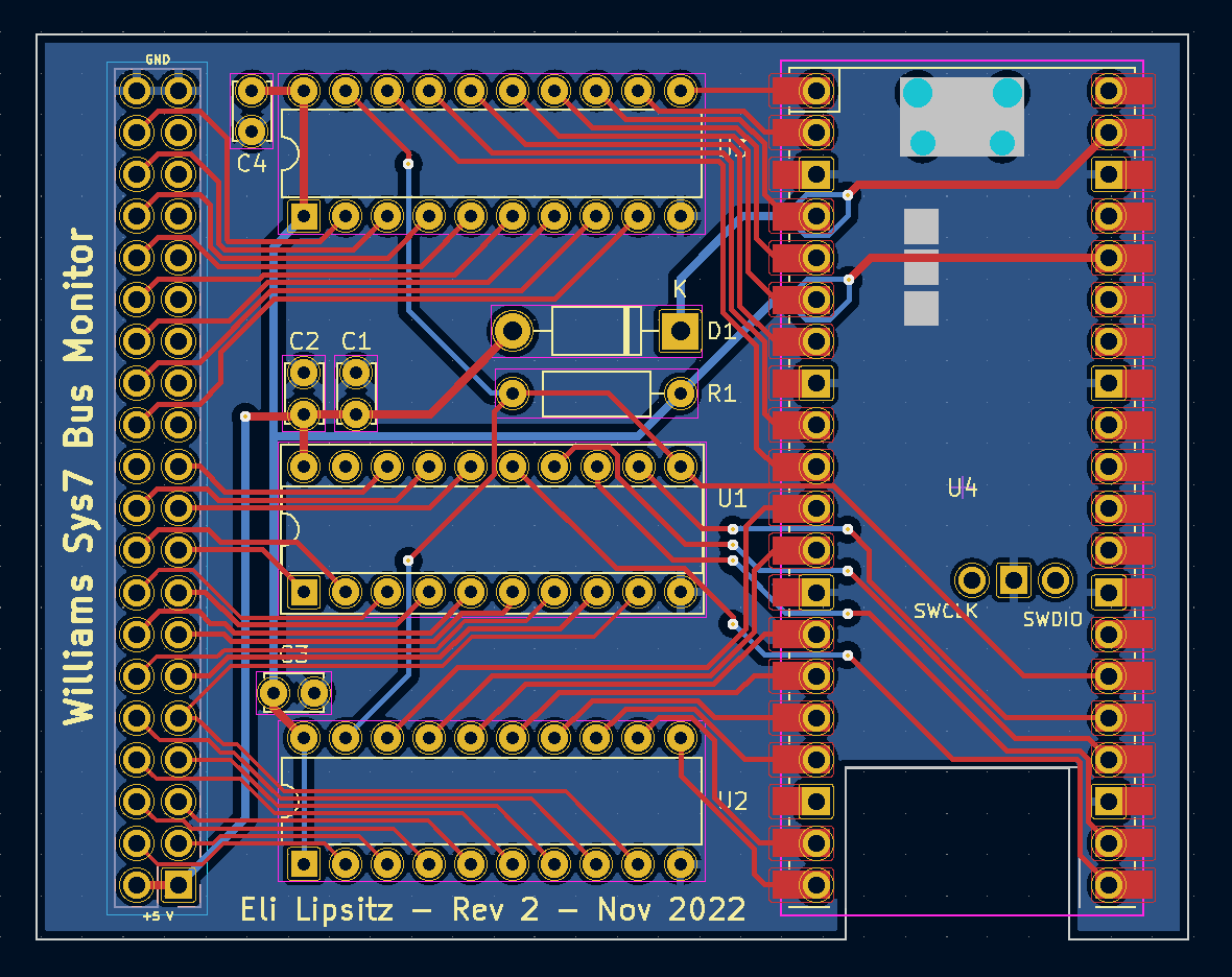
PCB revision 2, in KiCad
I ordered the new PCB and got to work on writing the device software.
Writing the initial software
I wrote the initial Pico prototypes in C, using the official C/C++ SDK. The SDK works pretty well, but doesn’t really have much for the Pico W (like an HTTP client, web server, OTA updates, etc). At this point I was getting a little sick of the project, so I looked for something that was a bit more batteries-included.
I was intrigued by Embassy, a fully async embedded framework written in Rust. Due to incomplete support for the Raspberry Pi Pico W, I ultimately settled on Arduino-Pico, an unofficial implementation of the Arduino API. The Arduino API is perhaps a bit oversimplified, and makes asynchronous I/O basically impossible, but the project had some very useful libraries built in which let me focus on the interesting parts. The Arduino IDE is abysmal, so I used VS Code with PlatformIO instead.
Pretty quickly I had a basic initial implementation of the device software. It was similar to the ESP32 version: core 1 was dedicated to interfacing with PIO. I probably could have used DMA to free up the core most of the time, but I didn’t end up needing to bother with it. Core 0 handled everything else. It connected to Wi-Fi on boot, hosted a status webpage, watched the shadow memory for a change in game state, and on game over, uploaded the scores from the shadow memory to a Flask webserver.
Installing the device
The PCB arrived and I assembled the new version of the device.
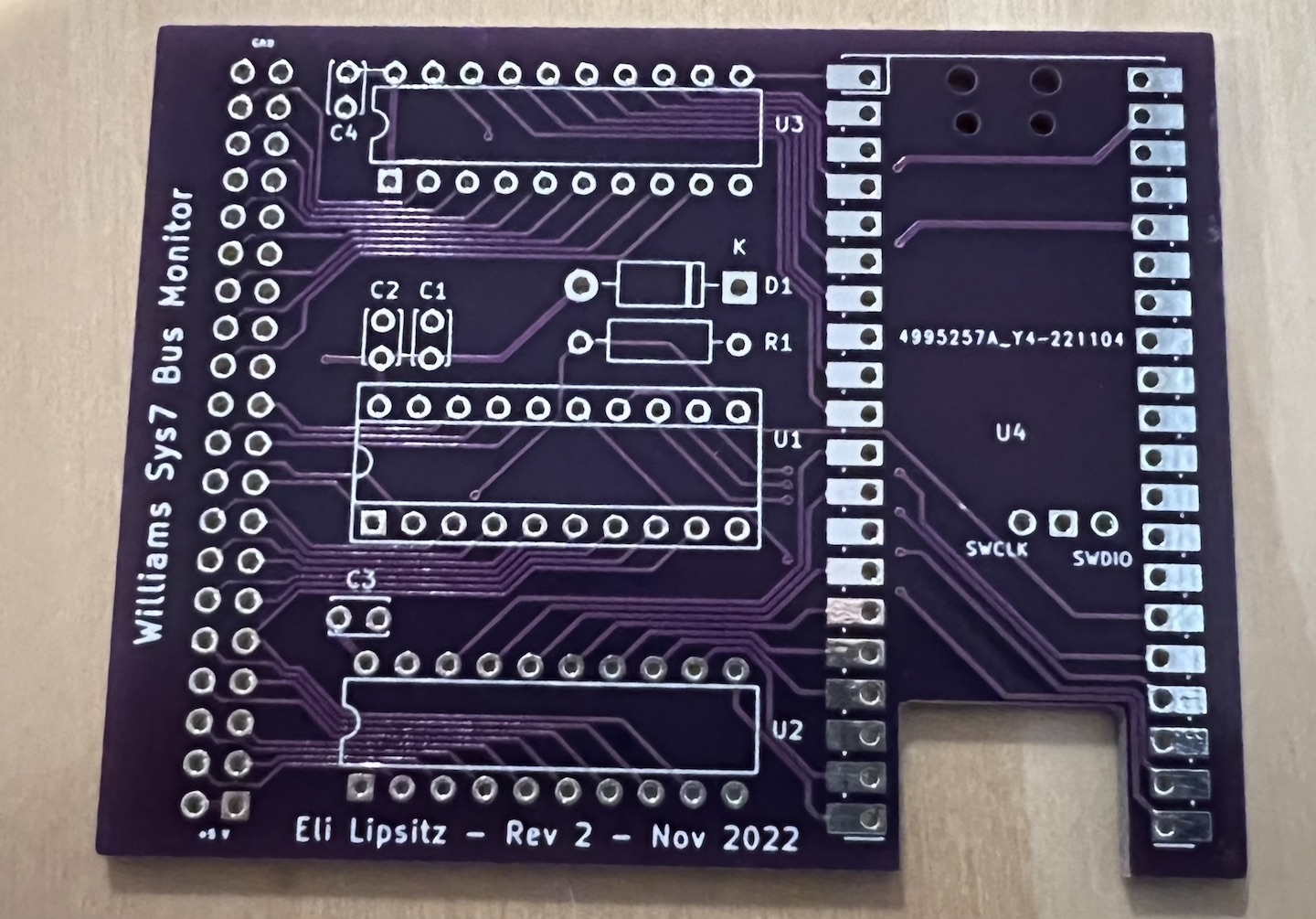
PCB revision 2, now in purple!
Next, I installed the pin header on the pinball machine’s MPU board. First, I had to remove the MPU board from the machine, which was a bit of a challenge. The MPU board is connected to another large circuit board (the “Driver board”) via a large, very important, and apparently unreliable connector. I opted to remove both boards together so I didn’t have to risk breaking the connector.
The boards are connected to the rest of the machine (display, switches, solenoids, sound, etc.) via eighteen different Molex connectors. They had become stiff over the past 40 years, so they were a little difficult to remove.
To solder in the 2x20 header, I first had to clear out the holes on the MPU board, which were plugged with solder. I used a braided copper solder wick to soak up the solder as I melted it, and then I soldered on the connector.
While the board was out, I removed the battery holder from the MPU board. The board needs 3x AA batteries to keep the CMOS RAM powered to maintain the high score list while the machine is off. I’d read that these batteries could sometimes leak onto the circuit board, causing substantial damage. To avoid this, I installed an enclosed battery pack that was connected to the MPU board by a long wire, so that the batteries would be located away from the MPU board if they ever leaked.
I screwed the boards back into the machine and carefully reconnected all of the Molex connectors. Then I turned the machine back on and… it didn’t work.
The display was showing what appeared to be an error message. I was afraid I had broken the machine, but I did some googling and realized that this was the expected behavior after the CMOS RAM loses power (when I replaced the batteries). The machine just needed to be reset with the coin door open, and then it started working again.
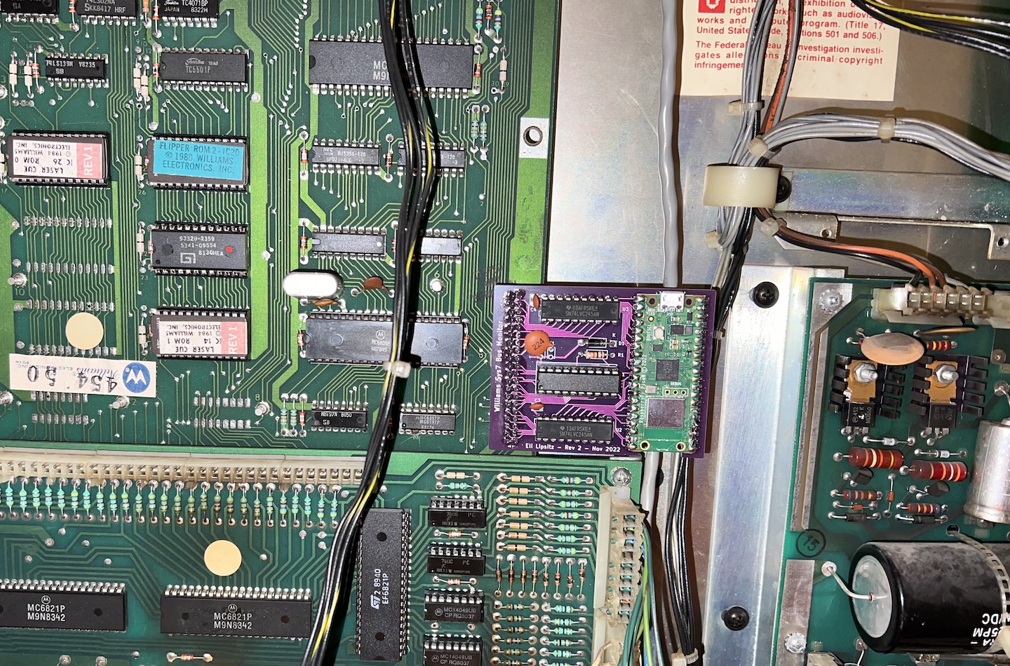
The device plugged into the pinball machine
I plugged in my board. It connected to Wi-Fi and I loaded the status webpage, which showed that the device wasn’t detecting any memory writes at all. I realized that while I had connected the “output enable” pin of the three chips to one of the RP2040 GPIOs, I forgot to actually turn it on. I fixed that and while the device still didn’t work, it was at least able to see the pins change.
I was worried that my trick of using the ATF16V8 to level-shift some of the signals, including the critical clock signal, didn’t actually work. I used a cheap logic analyzer directly on the MPU board and on my own board (downstream of the level shifters and ATF16V8) and confirmed that the signals were as I expected. I was a little bit stumped, but in the process of moving code around I got it to work.
I’m still not 100% sure what the issue was, but I think I wasn’t properly synchronizing the shared data between the two cores of the RP2040. Normally, I’d use atomic memory accesses (in this case, relaxed), but the RP2040 doesn’t have atomic instructions, so the libc excludes the atomics. Instead, I had to mark the shared memory as volatile to ensure that the compiler actually performed the writes so that the other core could see them.
After that software fix, the device worked! The device received the writes, at a rate of about 40K per second, so only 4% of clock cycles involved writes to RAM. I started up a new game of Laser Cue, and via manual inspection confirmed that the shadow memory on the device correctly reflected the scores in the game.
Finishing up the software
Once I got the core functionality of the device working, the rest of the project was relatively straightforward.
I implemented the functionality for the device to periodically poll the state of the shadow memory to determine when a game starts and ends. At the end of each ball I also snapshot the entire shadow memory to track the state of the game over time. Once the game ends, it uploads the memory snapshots to the webserver, which processes them to extract the score information.
If the device fails to upload the scores, it saves them locally on its flash storage, periodically re-attempting the upload. This ensures scores aren’t lost if the Wi-Fi drops or the score server goes down.
The web interface shows a simple table with scores, sortable by date and score. Clicking on a score displays a score breakdown for that game by player and ball. After the game ends, you can also “claim” a score by tapping on it and entering your initials.
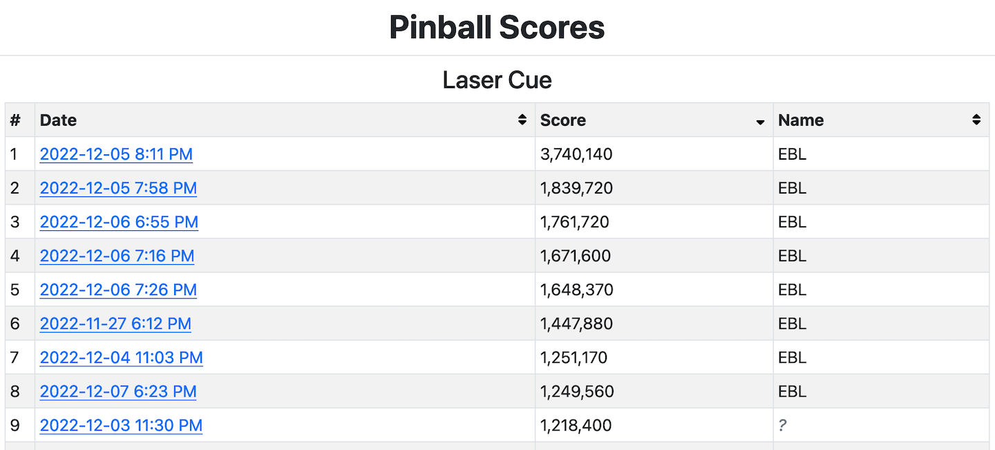
Score webpage, showing high scores
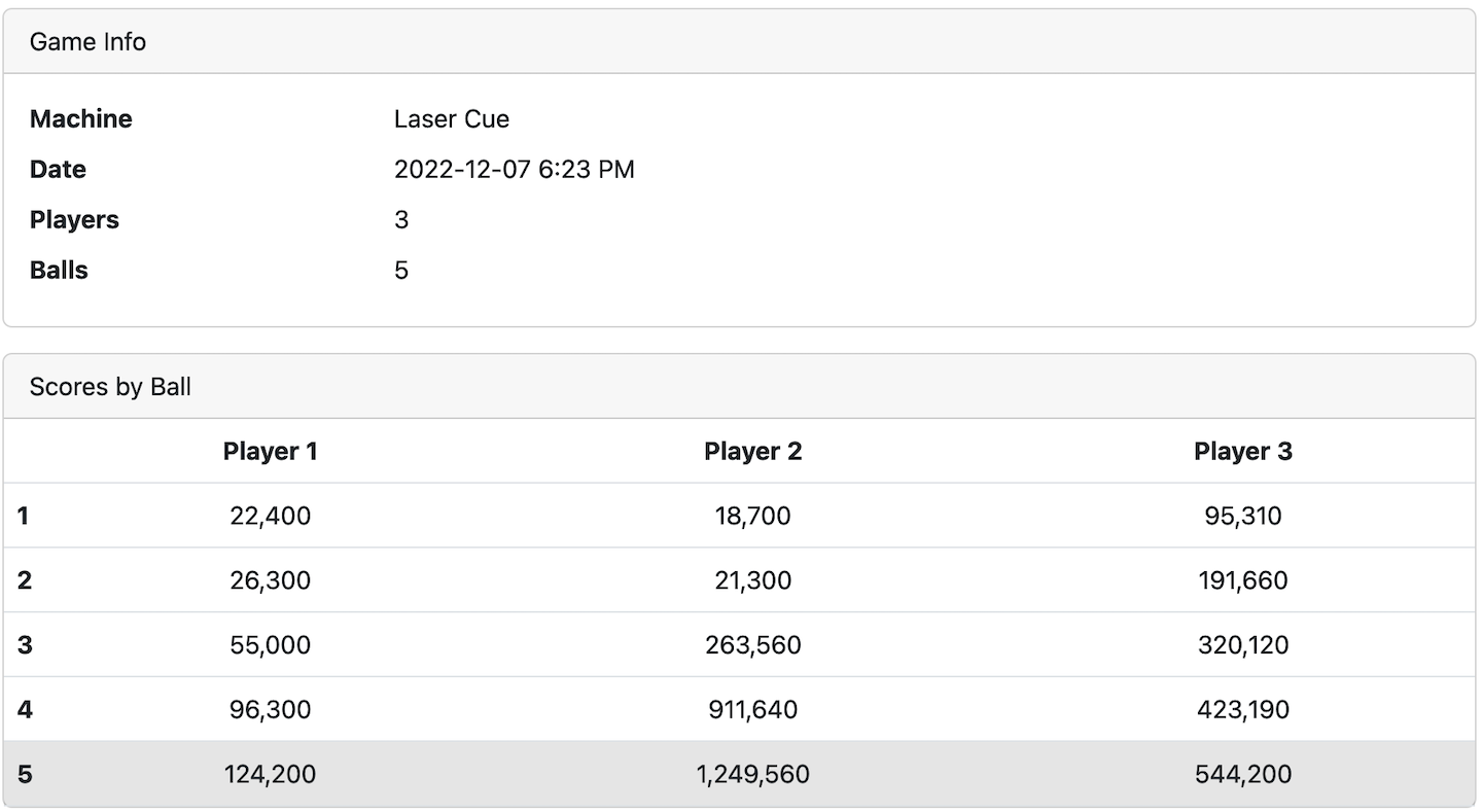
Score webpage, showing game detail page
Future work and retrospective
Overall, this was a really fun project. I learned some new skills (PCB design) and built a cool, somewhat useful toy.
There were a few things I wish I had done differently:
- Obviously, the ESP32-based solution didn’t work out, so I wish I had gone with the Raspberry Pi Pico W from the beginning.
- I should have just purchased a TL866II Plus to program the ATF16V8. It would have been a lot simpler than building the Afterburner device. Plus, it has some built-in logic testing capabilities.
- Adding more test points on the PCB. This is a pretty big one. When the device wasn’t working initially, I had a hard time attaching a probe to it — I had to solder pins on top of some contacts (not through a hole). If I had added some more unpopulated test points, it would have been a lot easier.
And a few things that I could maybe see myself doing in the future:
- Decoding more information from the game memory dump. Theoretically, I should be able to determine bonuses, which lights are lit, etc., and display that all on the score website.
- Live score display on the website. It probably doesn’t make sense for a home pinball machine, but it could be cool if the machine lived in an arcade or restaurant or something.
- Rewriting the controller using Embassy, a framework for embedded applications written in Rust. It looks pretty cool, and has support for the Pico / Pico W.
- Rewriting the device software to be more asynchronous and event driven. Right now, the Arduino-based approach heavily relies on blocking I/O. If I used something like FreeRTOS or Embassy, I’d be able to have a score uploader task, memory monitor task, debug server task, etc. all running simultaneously.
Acknowledgements
- PinWiki (and contributors) for the extensive information on the Williams System 7
- Jess Askey for the Williams System 7 Programming Guide. The memory map in particular was incredibly helpful.
- Arduino-Pico (Earle F. Philhower, III, and others), which helped get the device software up and running.
- I used a variety of open source software, including KiCad for PCB design, sigrok+PulseView for the logic analyzer, and Flask for the web interface.
- Williams, for creating Laser Cue and providing detailed schematics.